SCDS384A September 2018 – December 2018 TMUX6119
PRODUCTION DATA.
- 1 Features
- 2 Applications
- 3 Description
- 4 Revision History
- 5 Pin Configuration and Functions
-
6 Specifications
- 6.1 Absolute Maximum Ratings
- 6.2 ESD Ratings
- 6.3 Thermal Information
- 6.4 Recommended Operating Conditions
- 6.5 Electrical Characteristics (Dual Supplies: ±15 V)
- 6.6 Switching Characteristics (Dual Supplies: ±15 V)
- 6.7 Electrical Characteristics (Single Supply: 12 V)
- 6.8 Switching Characteristics (Single Supply: 12 V)
- 6.9 Typical Characteristics
- 7 Parameter Measurement Information
-
8 Detailed Description
- 8.1
Overview
- 8.1.1 On-Resistance
- 8.1.2 Off-Leakage Current
- 8.1.3 On-Leakage Current
- 8.1.4 Transition Time
- 8.1.5 Break-Before-Make Delay
- 8.1.6 Enable Turn-On and Enable Turn-Off Time
- 8.1.7 Charge Injection
- 8.1.8 Off Isolation
- 8.1.9 Channel-to-Channel Crosstalk
- 8.1.10 Bandwidth
- 8.1.11 THD + Noise
- 8.1.12 AC Power Supply Rejection Ratio (AC PSRR)
- 8.2 Functional Block Diagram
- 8.3 Feature Description
- 8.4 Device Functional Modes
- 8.1
Overview
- 9 Application and Implementation
- 10Power Supply Recommendations
- 11Layout
- 12Device and Documentation Support
- 13Mechanical, Packaging, and Orderable Information
Package Options
Mechanical Data (Package|Pins)
- DCN|8
Thermal pad, mechanical data (Package|Pins)
Orderable Information
8.1.1 On-Resistance
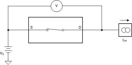
The on-resistance of the TMUX6119 is the ohmic resistance across the source (SA or SB) and drain (D) pins of the device. The on-resistance varies with input voltage and supply voltage. The symbol RON is used to denote on-resistance. The measurement setup used to measure RON is shown in Figure 17. Voltage (V) and current (ICH) are measured using this setup, and RON is computed as shown in Equation 1:
 Figure 17. On-Resistance Measurement Setup
 Equation 1. RON = V / ICH