SCDS431D October 2020 – July 2024 TMUX6211 , TMUX6212 , TMUX6213
PRODUCTION DATA
- 1
- 1 Features
- 2 Applications
- 3 Description
- 4 Device Comparison Table
- 5 Pin Configuration and Functions
-
6 Specifications
- 6.1 Absolute Maximum Ratings
- 6.2 ESD Ratings
- 6.3 Thermal Information
- 6.4 Recommended Operating Conditions
- 6.5 Source or Drain Continuous Current
- 6.6 ±15 V Dual Supply: Electrical Characteristics
- 6.7 ±15 V Dual Supply: Switching Characteristics
- 6.8 36 V Single Supply: Electrical Characteristics
- 6.9 36 V Single Supply: Switching Characteristics
- 6.10 12 V Single Supply: Electrical Characteristics
- 6.11 12 V Single Supply: Switching Characteristics
- 6.12 ±5 V Dual Supply: Electrical Characteristics
- 6.13 ±5 V Dual Supply: Switching Characteristics
- 6.14 Typical Characteristics
- 7 Parameter Measurement Information
- 8 Detailed Description
- 9 Application and Implementation
- 10Device and Documentation Support
- 11Revision History
- 12Mechanical, Packaging, and Orderable Information
Package Options
Mechanical Data (Package|Pins)
Thermal pad, mechanical data (Package|Pins)
- RUM|16
Orderable Information
3 Description
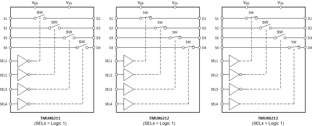
The TMUX6211, TMUX6212, and TMUX6213 are complementary metal-oxide semiconductor (CMOS) switches with four independently selectable 1:1, single-pole, single-throw (SPST) switch channels. The devices work with a single supply (4.5V to 36V), dual supplies (±4.5V to ±18V), or asymmetric supplies (such as VDD = 12V, VSS = –5V). The TMUX621x supports bidirectional analog and digital signals on the source (Sx) and drain (Dx) pins ranging from VSS to VDD.
The switches of the TMUX621x are controlled with appropriate logic control inputs on the SELx pins. The TMUX621x are part of the precision switches and multiplexers family of devices and have very low on and off leakage currents allowing them to be used in high precision measurement applications.
| PART NUMBER (1) | SWITCH | PACKAGE (2) |
|---|---|---|
| TMUX6211 | Logic Low | PW (TSSOP, 16) RUM (WQFN,16) |
| TMUX6212 | Logic High | |
| TMUX6213 | Logic Low + Logic High |
 TMUX621x Functional Block Diagrams