-
TMUX621x36V, Low-RON, 1:1 (SPST), 4-Channel Precision Switches with 1.8V Logic
- 1
- 1 Features
- 2 Applications
- 3 Description
- 4 Device Comparison Table
- 5 Pin Configuration and Functions
-
6 Specifications
- 6.1 Absolute Maximum Ratings
- 6.2 ESD Ratings
- 6.3 Thermal Information
- 6.4 Recommended Operating Conditions
- 6.5 Source or Drain Continuous Current
- 6.6 ±15 V Dual Supply: Electrical Characteristics
- 6.7 ±15 V Dual Supply: Switching Characteristics
- 6.8 36 V Single Supply: Electrical Characteristics
- 6.9 36 V Single Supply: Switching Characteristics
- 6.10 12 V Single Supply: Electrical Characteristics
- 6.11 12 V Single Supply: Switching Characteristics
- 6.12 ±5 V Dual Supply: Electrical Characteristics
- 6.13 ±5 V Dual Supply: Switching Characteristics
- 6.14 Typical Characteristics
- 7 Parameter Measurement Information
- 8 Detailed Description
- 9 Application and Implementation
- 10Device and Documentation Support
- 11Revision History
- 12Mechanical, Packaging, and Orderable Information
- IMPORTANT NOTICE
Package Options
Mechanical Data (Package|Pins)
Thermal pad, mechanical data (Package|Pins)
- RUM|16
Orderable Information
TMUX621x36V, Low-RON, 1:1 (SPST), 4-Channel Precision Switches with 1.8V Logic
1 Features
- Dual supply range: ±4.5V to ±18V
- Single supply range: 4.5V to 36V
- Low on-resistance: 2Ω
- High current support: 330mA (maximum) (WQFN)
- High current support: 220mA (maximum) (TSSOP)
- –40°C to +125°C operating temperature
- 1.8V logic compatible
- Integrated pull-down resistor on logic pins
- Fail-safe logic
- Rail-to-rail operation
- Bidirectional operation
2 Applications
- Sample-and-hold circuits
- Feedback gain switching
- Signal isolation
- Field transmitters
- Programmable logic controllers (PLC)
- Factory automation and control
- Ultrasound scanners
- Patient monitoring and diagnostics
- Electrocardiogram (ECG)
- Data acquisition systems (DAQ)
- Semiconductor test equipment
- LCD test
- Instrumentation: lab, analytical, portable
- Ultrasonic smart meters: water and gas
- Optical networking
- Optical test equipment
3 Description
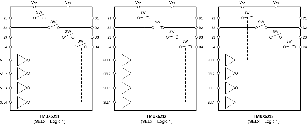
The TMUX6211, TMUX6212, and TMUX6213 are complementary metal-oxide semiconductor (CMOS) switches with four independently selectable 1:1, single-pole, single-throw (SPST) switch channels. The devices work with a single supply (4.5V to 36V), dual supplies (±4.5V to ±18V), or asymmetric supplies (such as VDD = 12V, VSS = –5V). The TMUX621x supports bidirectional analog and digital signals on the source (Sx) and drain (Dx) pins ranging from VSS to VDD.
The switches of the TMUX621x are controlled with appropriate logic control inputs on the SELx pins. The TMUX621x are part of the precision switches and multiplexers family of devices and have very low on and off leakage currents allowing them to be used in high precision measurement applications.
| PART NUMBER (1) | SWITCH | PACKAGE (2) |
|---|---|---|
| TMUX6211 | Logic Low | PW (TSSOP, 16) RUM (WQFN,16) |
| TMUX6212 | Logic High | |
| TMUX6213 | Logic Low + Logic High |
 TMUX621x Functional Block Diagrams
4 Device Comparison Table
| PRODUCT | DESCRIPTION | |
|---|---|---|
| TMUX6211 | Low-Leakage-Current, Precision, 4-Channel, 1:1 (SPST) Switches (Logic Low) | |
| TMUX6212 | Low-Leakage-Current, Precision, 4-Channel, 1:1 (SPST) Switches (Logic High) | |
| TMUX6213 | Low-Leakage-Current, Precision, 4-Channel, 1:1 (SPST) Switches (Logic Low + Logic High) | |
5 Pin Configuration and Functions
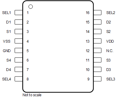
 Figure 5-1 PW Package 16-Pin TSSOP
Top View
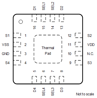
 Figure 5-2 RUM Package 16-Pin WQFN
Top View
Figure 5-2 RUM Package 16-Pin WQFN
Top View| PIN | TYPE(1) | DESCRIPTION(2) | ||
|---|---|---|---|---|
| NAME | TSSOP | WQFN | ||
| D1 | 2 | 16 | I/O | Drain pin 1. Can be an input or output. |
| D2 | 15 | 13 | I/O | Drain pin 2. Can be an input or output. |
| D3 | 10 | 8 | I/O | Drain pin 3. Can be an input or output. |
| D4 | 7 | 5 | I/O | Drain pin 4. Can be an input or output. |
| GND | 5 | 3 | P | Ground (0 V) reference |
| N.C. | 12 | 10 | — | No internal connection. Can be shorted to GND or left floating. |
| S1 | 3 | 1 | I/O | Source pin 1. Can be an input or output. |
| S2 | 14 | 12 | I/O | Source pin 2. Can be an input or output. |
| S3 | 11 | 9 | I/O | Source pin 3. Can be an input or output. |
| S4 | 6 | 4 | I/O | Source pin 4. Can be an input or output. |
| S3 | 11 | 9 | I/O | Source pin 3. Can be an input or output. |
| SEL1 | 1 | 15 | I | Logic control input 1, has internal 4 MΩ pull-down resistor. Controls channel 1 state as shown in Section 8.5. |
| SEL2 | 16 | 14 | I | Logic control input 2, has internal 4 MΩ pull-down resistor. Controls channel 2 state as shown in Section 8.5. |
| SEL3 | 9 | 7 | I | Logic control input 3, has internal 4 MΩ pull-down resistor. Controls channel 3 state as shown in Section 8.5. |
| SEL4 | 8 | 6 | I | Logic control input 4, has internal 4 MΩ pull-down resistor. Controls channel 4 state as shown in Section 8.5. |
| VDD | 13 | 11 | P | Positive power supply. This pin is the most positive power-supply potential. For reliable operation, connect a decoupling capacitor ranging from 0.1 µF to 10 µF between VDD and GND. |
| VSS | 4 | 2 | P | Negative power supply. This pin is the most negative power-supply potential. In single-supply applications, this pin can be connected to ground. For reliable operation, connect a decoupling capacitor ranging from 0.1 μF to 10 μF between VSS and GND. |
| Thermal Pad | — | The thermal pad is not connected internally. No requirement to solder this pad, if connected it is recommended that the pad be left floating or tied to GND | ||