SCDS431D October 2020 – July 2024 TMUX6211 , TMUX6212 , TMUX6213
PRODUCTION DATA
- 1
- 1 Features
- 2 Applications
- 3 Description
- 4 Device Comparison Table
- 5 Pin Configuration and Functions
-
6 Specifications
- 6.1 Absolute Maximum Ratings
- 6.2 ESD Ratings
- 6.3 Thermal Information
- 6.4 Recommended Operating Conditions
- 6.5 Source or Drain Continuous Current
- 6.6 ±15 V Dual Supply: Electrical Characteristics
- 6.7 ±15 V Dual Supply: Switching Characteristics
- 6.8 36 V Single Supply: Electrical Characteristics
- 6.9 36 V Single Supply: Switching Characteristics
- 6.10 12 V Single Supply: Electrical Characteristics
- 6.11 12 V Single Supply: Switching Characteristics
- 6.12 ±5 V Dual Supply: Electrical Characteristics
- 6.13 ±5 V Dual Supply: Switching Characteristics
- 6.14 Typical Characteristics
- 7 Parameter Measurement Information
- 8 Detailed Description
- 9 Application and Implementation
- 10Device and Documentation Support
- 11Revision History
- 12Mechanical, Packaging, and Orderable Information
Package Options
Mechanical Data (Package|Pins)
Thermal pad, mechanical data (Package|Pins)
- RUM|16
Orderable Information
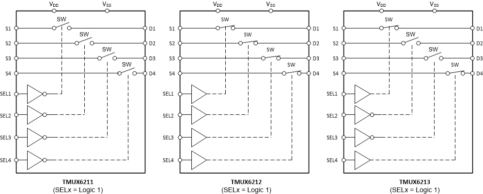
8.2 Functional Block Diagram
