SCDS431D October 2020 – July 2024 TMUX6211 , TMUX6212 , TMUX6213
PRODUCTION DATA
- 1
- 1 Features
- 2 Applications
- 3 Description
- 4 Device Comparison Table
- 5 Pin Configuration and Functions
-
6 Specifications
- 6.1 Absolute Maximum Ratings
- 6.2 ESD Ratings
- 6.3 Thermal Information
- 6.4 Recommended Operating Conditions
- 6.5 Source or Drain Continuous Current
- 6.6 ±15 V Dual Supply: Electrical Characteristics
- 6.7 ±15 V Dual Supply: Switching Characteristics
- 6.8 36 V Single Supply: Electrical Characteristics
- 6.9 36 V Single Supply: Switching Characteristics
- 6.10 12 V Single Supply: Electrical Characteristics
- 6.11 12 V Single Supply: Switching Characteristics
- 6.12 ±5 V Dual Supply: Electrical Characteristics
- 6.13 ±5 V Dual Supply: Switching Characteristics
- 6.14 Typical Characteristics
- 7 Parameter Measurement Information
- 8 Detailed Description
- 9 Application and Implementation
- 10Device and Documentation Support
- 11Revision History
- 12Mechanical, Packaging, and Orderable Information
Package Options
Mechanical Data (Package|Pins)
Thermal pad, mechanical data (Package|Pins)
- RUM|16
Orderable Information
5 Pin Configuration and Functions
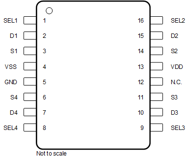
 Figure 5-1 PW Package 16-Pin TSSOP
Top View
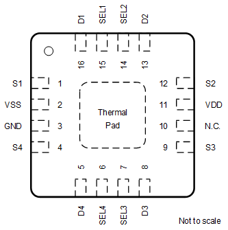
 Figure 5-2 RUM Package 16-Pin WQFN
Top View
Figure 5-2 RUM Package 16-Pin WQFN
Top ViewTable 5-1 Pin Functions
| PIN | TYPE(1) | DESCRIPTION(2) | ||
|---|---|---|---|---|
| NAME | TSSOP | WQFN | ||
| D1 | 2 | 16 | I/O | Drain pin 1. Can be an input or output. |
| D2 | 15 | 13 | I/O | Drain pin 2. Can be an input or output. |
| D3 | 10 | 8 | I/O | Drain pin 3. Can be an input or output. |
| D4 | 7 | 5 | I/O | Drain pin 4. Can be an input or output. |
| GND | 5 | 3 | P | Ground (0 V) reference |
| N.C. | 12 | 10 | — | No internal connection. Can be shorted to GND or left floating. |
| S1 | 3 | 1 | I/O | Source pin 1. Can be an input or output. |
| S2 | 14 | 12 | I/O | Source pin 2. Can be an input or output. |
| S3 | 11 | 9 | I/O | Source pin 3. Can be an input or output. |
| S4 | 6 | 4 | I/O | Source pin 4. Can be an input or output. |
| S3 | 11 | 9 | I/O | Source pin 3. Can be an input or output. |
| SEL1 | 1 | 15 | I | Logic control input 1, has internal 4 MΩ pull-down resistor. Controls channel 1 state as shown in Section 8.5. |
| SEL2 | 16 | 14 | I | Logic control input 2, has internal 4 MΩ pull-down resistor. Controls channel 2 state as shown in Section 8.5. |
| SEL3 | 9 | 7 | I | Logic control input 3, has internal 4 MΩ pull-down resistor. Controls channel 3 state as shown in Section 8.5. |
| SEL4 | 8 | 6 | I | Logic control input 4, has internal 4 MΩ pull-down resistor. Controls channel 4 state as shown in Section 8.5. |
| VDD | 13 | 11 | P | Positive power supply. This pin is the most positive power-supply potential. For reliable operation, connect a decoupling capacitor ranging from 0.1 µF to 10 µF between VDD and GND. |
| VSS | 4 | 2 | P | Negative power supply. This pin is the most negative power-supply potential. In single-supply applications, this pin can be connected to ground. For reliable operation, connect a decoupling capacitor ranging from 0.1 μF to 10 μF between VSS and GND. |
| Thermal Pad | — | The thermal pad is not connected internally. No requirement to solder this pad, if connected it is recommended that the pad be left floating or tied to GND | ||
(1) I = input, O = output, I/O = input and output, P = power.
(2) Refer to Section 8.4 for what to do with
unused pins.