SCDS416D October 2020 – July 2024 TMUX7211 , TMUX7212 , TMUX7213
PRODUCTION DATA
- 1
- 1 Features
- 2 Applications
- 3 Description
- 4 Device Comparison Table
- 5 Pin Configuration and Functions
-
6 Specifications
- 6.1 Absolute Maximum Ratings
- 6.2 ESD Ratings
- 6.3 Thermal Information
- 6.4 Recommended Operating Conditions
- 6.5 Source or Drain Continuous Current
- 6.6 ±15 V Dual Supply: Electrical Characteristics
- 6.7 ±15 V Dual Supply: Switching Characteristics
- 6.8 ±20 V Dual Supply: Electrical Characteristics
- 6.9 ±20 V Dual Supply: Switching Characteristics
- 6.10 44 V Single Supply: Electrical Characteristics
- 6.11 44 V Single Supply: Switching Characteristics
- 6.12 12 V Single Supply: Electrical Characteristics
- 6.13 12 V Single Supply: Switching Characteristics
- 6.14 Typical Characteristics
- 7 Parameter Measurement Information
- 8 Detailed Description
- 9 Application and Implementation
- 10Device and Documentation Support
- 11Revision History
- 12Mechanical, Packaging, and Orderable Information
Package Options
Mechanical Data (Package|Pins)
Thermal pad, mechanical data (Package|Pins)
- RUM|16
Orderable Information
3 Description
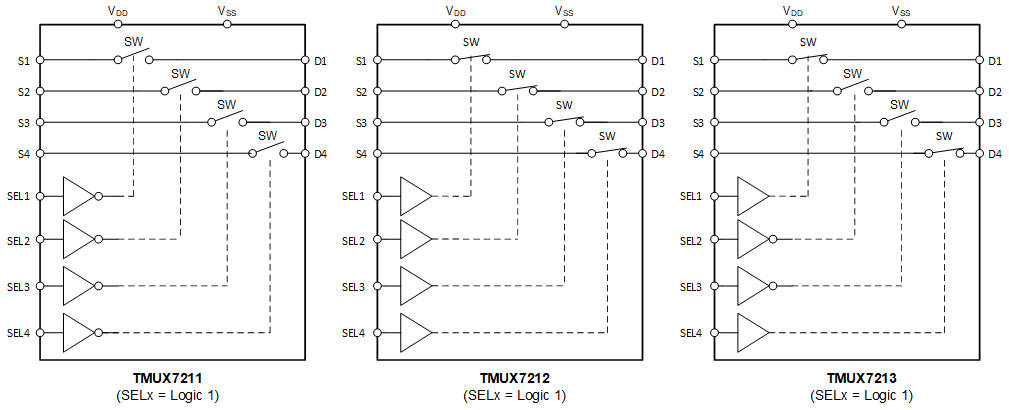
The TMUX7212 is a complementary metal-oxide semiconductor (CMOS) switch with four independently selectable 1:1, single-pole, single-throw (SPST) switch channels. This device works with a single supply (4.5V to 44V), dual supplies (±4.5V to ±22V), or asymmetric supplies (such as VDD = 12V, VSS = –5V). The TMUX721x supports bidirectional analog and digital signals on the source (Sx) and drain (Dx) pins ranging from VSS to VDD.
The switches of the TMUX721x are controlled with appropriate logic control inputs on the SELx pins. The TMUX721x is part of the precision switches and multiplexers family of devices and has very low on and off leakage currents allowing them to be used in high precision measurement applications.
The TMUX721x provides latch-up immunity, preventing undesirable high current events between parasitic structures within the device typically caused by overvoltage events. A latch-up condition typically continues until the power supply rails are turned off and can lead to device failure. The latch-up immunity feature allows the TMUX721x to be used in harsh environments.
| PART NUMBER (1) | ACTIVE LOGIC | PACKAGE (2) |
|---|---|---|
| TMUX7211 | Logic Low | PW (TSSOP, 16) RUM (WQFN, 16) |
| TMUX7212 | Logic High | |
| TMUX7213 | Logic Low + Logic High |
 TMUX721x Functional Block Diagram