SCDS416D October 2020 – July 2024 TMUX7211 , TMUX7212 , TMUX7213
PRODUCTION DATA
- 1
- 1 Features
- 2 Applications
- 3 Description
- 4 Device Comparison Table
- 5 Pin Configuration and Functions
-
6 Specifications
- 6.1 Absolute Maximum Ratings
- 6.2 ESD Ratings
- 6.3 Thermal Information
- 6.4 Recommended Operating Conditions
- 6.5 Source or Drain Continuous Current
- 6.6 ±15 V Dual Supply: Electrical Characteristics
- 6.7 ±15 V Dual Supply: Switching Characteristics
- 6.8 ±20 V Dual Supply: Electrical Characteristics
- 6.9 ±20 V Dual Supply: Switching Characteristics
- 6.10 44 V Single Supply: Electrical Characteristics
- 6.11 44 V Single Supply: Switching Characteristics
- 6.12 12 V Single Supply: Electrical Characteristics
- 6.13 12 V Single Supply: Switching Characteristics
- 6.14 Typical Characteristics
- 7 Parameter Measurement Information
- 8 Detailed Description
- 9 Application and Implementation
- 10Device and Documentation Support
- 11Revision History
- 12Mechanical, Packaging, and Orderable Information
Package Options
Mechanical Data (Package|Pins)
Thermal pad, mechanical data (Package|Pins)
- RUM|16
Orderable Information
7.7 Charge Injection
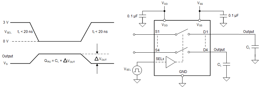
The TMUX721x devices have a transmission-gate topology. Any mismatch in capacitance between the NMOS and PMOS transistors results in a charge injected into the drain or source during the falling or rising edge of the gate signal. The amount of charge injected into the source or drain of the device is known as charge injection, and is denoted by the symbol QC. Figure 7-7 shows the setup used to measure charge injection from source (Sx) to drain (Dx).
 Figure 7-7 Charge-Injection Measurement
Setup