SCDS438C January 2021 – December 2024 TMUX7219-Q1
PRODUCTION DATA
- 1
- 1 Features
- 2 Applications
- 3 Description
- 4 Pin Configuration and Functions
-
5 Specifications
- 5.1 Absolute Maximum Ratings
- 5.2 ESD Ratings
- 5.3 Thermal Information
- 5.4 Recommended Operating Conditions
- 5.5 Source or Drain Continuous Current
- 5.6 ±15 V Dual Supply: Electrical Characteristics
- 5.7 ±15 V Dual Supply: Switching Characteristics
- 5.8 ±20 V Dual Supply: Electrical Characteristics
- 5.9 ±20 V Dual Supply: Switching Characteristics
- 5.10 44 V Single Supply: Electrical Characteristics
- 5.11 44 V Single Supply: Switching Characteristics
- 5.12 12 V Single Supply: Electrical Characteristics
- 5.13 12 V Single Supply: Switching Characteristics
- 5.14 Typical Characteristics
-
6 Parameter Measurement Information
- 6.1 On-Resistance
- 6.2 Off-Leakage Current
- 6.3 On-Leakage Current
- 6.4 Transition Time
- 6.5 tON(EN) and tOFF(EN)
- 6.6 Break-Before-Make
- 6.7 tON (VDD) Time
- 6.8 Propagation Delay
- 6.9 Charge Injection
- 6.10 Off Isolation
- 6.11 Crosstalk
- 6.12 Bandwidth
- 6.13 THD + Noise
- 6.14 Power Supply Rejection Ratio (PSRR)
- 7 Detailed Description
- 8 Application and Implementation
- 9 Device and Documentation Support
- 10Revision History
- 11Mechanical, Packaging, and Orderable Information
Package Options
Mechanical Data (Package|Pins)
- DGK|8
Thermal pad, mechanical data (Package|Pins)
Orderable Information
3 Description
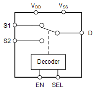
The TMUX7219-Q1 is a complementary metal-oxide semiconductor (CMOS) switch with latch-up immunity in a single channel, 2:1 (SPDT) configuration. The device works with a single supply (4.5V to 44V), dual supplies (±4.5V to ±22V), or asymmetric supplies (such as VDD = 12V, VSS = –5V). The TMUX7219-Q1 supports bidirectional analog and digital signals on the source (Sx) and drain (D) pins ranging from VSS to VDD.
The TMUX7219-Q1 can be enabled or disabled by controlling the EN pin. When disabled, both signal path switches are off. When enabled, the SEL pin can be used to turn on signal path 1 (S1 to D) or signal path 2 (S2 to D). All logic control inputs support logic levels from 1.8V to VDD, ensuring both TTL and CMOS logic compatibility when operating in the valid supply voltage range. Fail-Safe Logic circuitry allows voltages on the control pins to be applied before the supply pin, protecting the device from potential damage.
The TMUX72xx family provides latch-up immunity, preventing undesirable high current events between parasitic structures within the device typically caused by overvoltage events. A latch-up condition typically continues until the power supply rails are turned off and can lead to device failure. The latch-up immunity feature allows the TMUX72xx family of switches and multiplexers to be used in harsh environments.
| PART NUMBER | PACKAGE (1) | BODY SIZE (NOM) |
|---|---|---|
| TMUX7219-Q1 | VSSOP (8) DGK | 3.00mm × 3.00mm |
 Functional Block
Diagram