SCDS404B March 2021 – November 2022 TMUX7411F , TMUX7412F , TMUX7413F
PRODMIX
- 1 Features
- 2 Applications
- 3 Description
- 4 Revision History
- 5 Device Comparison Table
- 6 Pin Configuration and Functions
-
7 Specifications
- 7.1 Absolute Maximum Ratings
- 7.2 ESD Ratings
- 7.3 Thermal Information
- 7.4 Recommended Operating Conditions
- 7.5 Electrical Characteristics: Global
- 7.6 ±15 V Dual Supply: Electrical Characteristics
- 7.7 ±20 V Dual Supply: Electrical Characteristics
- 7.8 12 V Single Supply: Electrical Characteristics
- 7.9 36 V Single Supply: Electrical Characteristics
- 7.10 Typical Characteristics
-
8 Parameter Measurement Information
- 8.1 On-Resistance
- 8.2 Turn-On and Turn-Off Time
- 8.3 Off-Leakage Current
- 8.4 On-Leakage Current
- 8.5 Input and Output Leakage Current Under Overvoltage Fault
- 8.6 Fault Response Time
- 8.7 Fault Recovery Time
- 8.8 Fault Flag Response Time
- 8.9 Fault Flag Recovery Time
- 8.10 Charge Injection
- 8.11 Off Isolation
- 8.12 Inter-Channel Crosstalk
- 8.13 Bandwidth
- 8.14 THD + Noise
- 9 Detailed Description
- 10Application and Implementation
- 11Power Supply Recommendations
- 12Layout
- 13Device and Documentation Support
- 14Mechanical, Packaging, and Orderable Information
Package Options
Mechanical Data (Package|Pins)
- RRP|16
Thermal pad, mechanical data (Package|Pins)
Orderable Information
8.1 On-Resistance
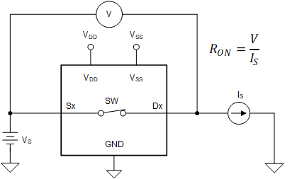
The on-resistance of the TMUX7411F, TMUX7412F, and TMUX7413F is the ohmic resistance across the source (Sx) and drain (Dx) pins of the device. The on-resistance varies with input voltage and supply voltage. The symbol RON is used to denote on-resistance. Figure 8-1 shows the measurement setup used to measure RON. ΔRON represents the difference between the RON of any two channels, while RON_FLAT denotes the flatness that is defined as the difference between the maximum and minimum value of on-resistance measured over the specified analog signal range.
 Figure 8-1 On-Resistance Measurement Setup