SLOS275E January 2000 – November 2016 TPA0211
PRODUCTION DATA.
- 1 Features
- 2 Applications
- 3 Description
- 4 Revision History
- 5 Device Comparison Table
- 6 Pin Configuration and Functions
- 7 Specifications
- 8 Parameter Measurement Information
- 9 Detailed Description
- 10Application and Implementation
- 11Power Supply Recommendations
- 12Layout
- 13Device and Documentation Support
- 14Mechanical, Packaging, and Orderable Information
Package Options
Refer to the PDF data sheet for device specific package drawings
Mechanical Data (Package|Pins)
- DGN|8
Thermal pad, mechanical data (Package|Pins)
- DGN|8
Orderable Information
9 Detailed Description
9.1 Overview
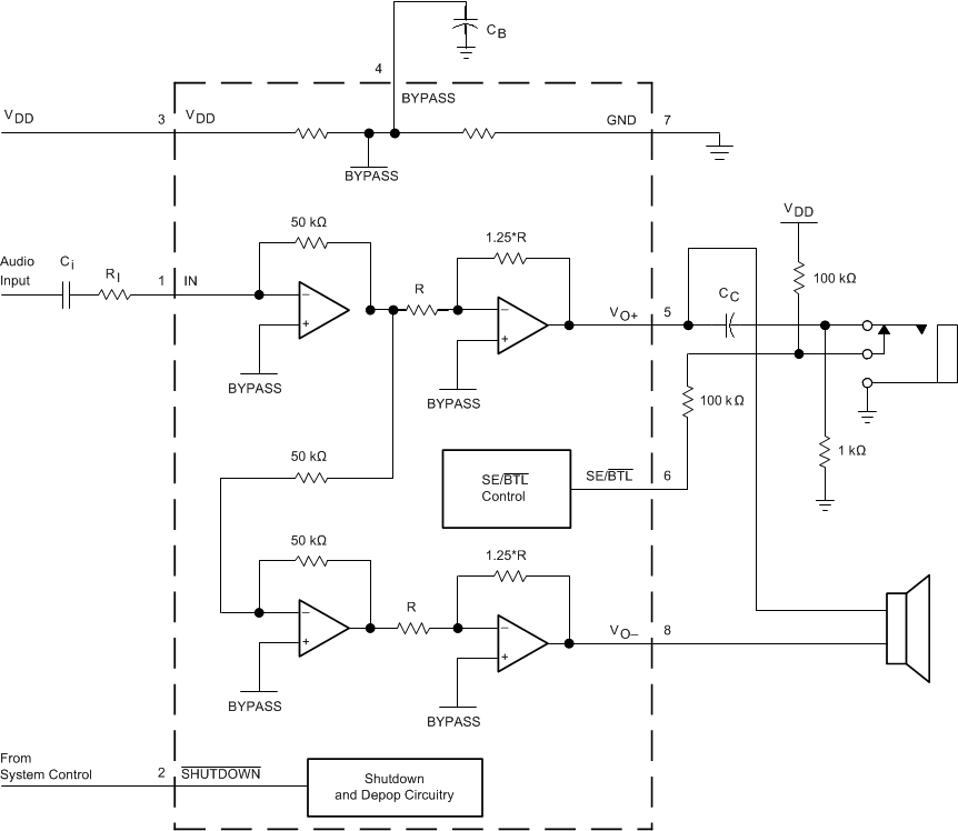
The TPA0211 device is a Class AB audio power amplifier designed to drive speakers in applications like small wireless communicators, cellphones, notebooks, and so forth. The TPA0211 can deliver 2 W (1% THD+N) of power into a 4-Ω speaker.
This device is available in the 8-pin thermally-enhanced MSOP-PowerPAD package (DGN) and operates over an ambient temperature range of –40°C to 85°C.
9.2 Functional Block Diagram
9.3 Feature Description
9.3.1 Bridged-Tied Load Versus Single-Ended Mode
Figure 23 shows a Class-AB audio power amplifier (APA) in a BTL configuration. The TPA0211 BTL amplifier consists of two Class-AB amplifiers driving both ends of the load. There are several potential benefits to this differential drive configuration, but initially consider power to the load. The differential drive to the speaker means that as one side is slewing up, the other side is slewing down, and vice versa. This, in effect, doubles the voltage swing on the load as compared to a ground referenced load. Plugging 2 × VO(PP) into the power equation, where voltage is squared, yields 4 times the output power from the same supply rail and load impedance (see Equation 1 and ).
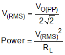
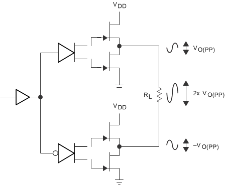 Figure 23. Bridge-Tied Load Configuration
In a typical computer sound channel operating at 5 V, bridging raises the power into an 8-Ω speaker from a singled-ended (SE, ground reference) limit of 250 mW to 1 W. In sound power, that is a 6-dB improvement — which is loudness that can be heard. In addition to increased power, there are frequency response concerns. Consider the single-supply SE configuration shown in Figure 24. A coupling capacitor is required to block the dc offset voltage from reaching the load. These capacitors can be quite large (approximately 33 µF to 1000 µF) so they tend to be expensive, heavy, occupy valuable PCB area, and have the additional drawback of limiting low-frequency performance of the system. This frequency limiting effect is due to the high pass filter network created with the speaker impedance and the coupling capacitance and is calculated with Equation 2.
 )
)For example, a 68-µF capacitor with an 8-Ω speaker would attenuate low frequencies below 293 Hz. The BTL configuration cancels the dc offsets, which eliminates the need for the blocking capacitors. Low-frequency performance is then limited only by the input network and speaker response. Cost and PCB space are also minimized by eliminating the bulky coupling capacitor.
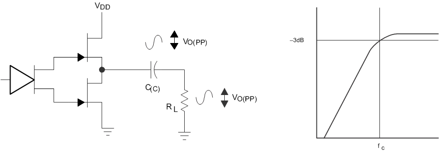 Figure 24. Single-Ended Configuration and Frequency Response
Increasing power to the load does carry a penalty of increased internal power dissipation. The increased dissipation is understandable considering that the BTL configuration produces 4 times the output power of the SE configuration. Internal dissipation versus output power is discussed further in Crest Factor.
9.3.2 Single-Ended Operation
In SE mode (see Figure 23 and Figure 24), the load is driven from one amplifier output (VO+, terminal 5).
The amplifier switches to single-ended operation when the SE/BTL terminal is held high.
9.3.3 BTL Amplifier Efficiency
Class-AB amplifiers are inefficient. The primary cause of inefficiencies is the voltage drop across the output stage transistors. There are two components of the internal voltage drop. One is the headroom or dc voltage drop that varies inversely to output power. The second component is due to the sinewave nature of the output. The total voltage drop can be calculated by subtracting the RMS value of the output voltage from VDD. The internal voltage drop multiplied by the RMS value of the supply current, IDDrms, determines the internal power dissipation of the amplifier.
An easy-to-use equation to calculate efficiency starts out as being equal to the ratio of power from the power supply to the power delivered to the load. To accurately calculate the RMS and average values of power in the load and in the amplifier, the current and voltage waveform shapes must first be understood (see Figure 25).
 Figure 25. Voltage and Current Waveforms for BTL Amplifiers
Although the voltages and currents for SE and BTL are sinusoidal in the load, currents from the supply are very different between SE and BTL configurations. In an SE application the current waveform is a half-wave rectified shape, whereas in BTL it is a full-wave rectified waveform. This means RMS conversion factors are different. Keep in mind that for most of the waveform both the push and pull transistors are not on at the same time, which supports the fact that each amplifier in the BTL device only draws current from the supply for half the waveform. Equation 3 and Equation 4 are the basis for calculating amplifier efficiency.
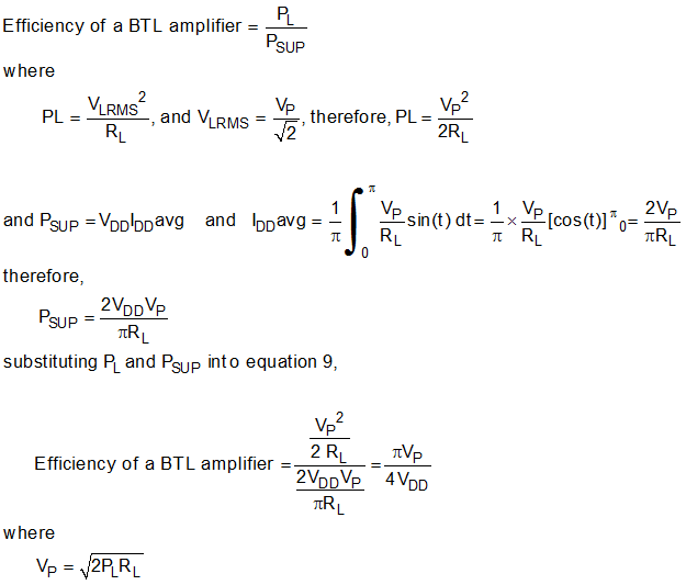

Table 2 employs Equation 3 to calculate efficiencies for four different output power levels. Note that the efficiency of the amplifier is quite low for lower power levels and rises sharply as power to the load is increased resulting in a nearly flat internal power dissipation over the normal operating range. Note that the internal dissipation at full output power is less than in the half power range. Calculating the efficiency for a specific system is the key to proper power supply design.
Table 2. Efficiency vs Output Power in 5-V 8-Ω BTL Systems
| OUTPUT POWER (W) | EFFICIENCY (%) | PEAK VOLTAGE (V) | INTERNAL DISSIPATION (W) |
|---|---|---|---|
| 0.25 | 31.4 | 2 | 0.55 |
| 0.5 | 44.4 | 2.83 | 0.62 |
| 1 | 62.8 | 4 | 0.59 |
| 1.25 | 70.2 | 4.47(1) | 0.53 |
A final point to remember about Class-AB amplifiers (either SE or BTL) is how to manipulate the terms in the efficiency equation to utmost advantage when possible. Note that in Equation 3, VDD is in the denominator. This indicates that as VDD goes down, efficiency goes up.
9.3.4 Gain Setting Via Input Resistance
The gain of the input stage is set by the user-selected input resistor and a 50-kΩ internal feedback resistor.
However, the power stage is internally configured with a gain of –1.25 V/V in SE mode, and –2.5 V/V in BTL mode. Thus, the feedback resistor (RF) is effectively 62.5 kΩ in SE mode and 125 kΩ in BTL mode. Therefore, the overall gain can be calculated using Equation 5 and Equation 6.

 (SE)
(SE)The –3 dB frequency can be calculated using Equation 7.

If the filter must be more accurate, the value of the capacitor should be increased while the value of the resistor to ground should be decreased. In addition, the order of the filter could be increased.
9.3.5 Crest Factor
Class-AB power amplifiers dissipate a significant amount of heat in the package under normal operating conditions. A typical music CD requires 12 dB to 15 dB of dynamic range, or headroom above the average power output, to pass the loudest portions of the signal without distortion. In other words, music typically has a crest factor between 12 dB and 15 dB. When determining the optimal ambient operating temperature, the internal dissipated power at the average output power level must be used. The TPA0211 data sheet shows that when the TPA0211 is operating from a 5-V supply into a 4-Ω speaker 4-W peaks are available. Converting watts to dB with Equation 8.

Converting dB back into watts with Equation 9.
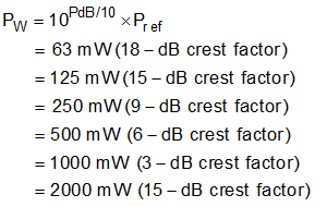
This is valuable information to consider when attempting to estimate the heat dissipation requirements for the amplifier system. Comparing the absolute worst case, which is 2 W of continuous power output with a 3 dB crest factor, against 12 dB and 15 dB applications drastically affects maximum ambient temperature ratings for the system. Table 3 shows maximum ambient temperatures and TPA0211 internal power dissipation for various output-power levels.
Table 3. TPA0211 Power Rating, 5-V, 4–Ω, Mono
| PEAK OUTPUT POWER (W) | AVERAGE OUTPUT POWER | POWER DISSIPATION (W) | MAXIMUM AMBIENT TEMPERATURE |
|---|---|---|---|
| 4 | 2 W (3-dB crest factor) | 1.7 | –3°C |
| 4 | 1000 mW (6-dB crest factor) | 1.6 | 6°C |
| 4 | 500 mW (9-dB crest factor) | 1.4 | 24°C |
| 4 | 250 mW (12-dB crest factor) | 1.1 | 51°C |
| 4 | 125 mW (15-dB crest factor) | 0.8 | 78°C |
| 4 | 63 mW (18-dB crest factor) | 0.6 | 96°C |
As a result, Equation 10 for calculating PDmax may be used for an 4-Ω application.

However, in the case of a 4-Ω load, the PDmax occurs at a point well above the normal operating power level. The amplifier may therefore be operated at a higher ambient temperature than required by the PDmax formula for a 4-Ω load.
9.4 Device Functional Modes
9.4.1 Shutdown Mode
The TPA0211 amplifier can be put in shutdown mode when asserting shutdown pin to a logic LOW. While in shutdown mode, the device output stage is turned off and the current consumption is very low.
9.4.2 SE/BTL (Stereo/Mono) Operation
The ability of the TPA0211 to easily switch between mono BTL and stereo SE modes is one of its most important cost saving features. This feature eliminates the requirement for an additional headphone amplifier in applications where an internal speaker is driven in BTL mode but an external headphone must be accommodated. When SE/BTL is held high for SE mode, the VO– output goes into a high impedance state while the VO+ output operates normally. When SE/BTL is held low, the VO– output operates normally, placing the amplifier in BTL mode.
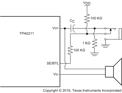 Figure 26. TPA0211 Resistor Divider Network Circuit
Using a readily available 1/8-in (3.5 mm) mono headphone jack, the control switch is closed when no plug is inserted. When closed, the 100-kΩ, 1-kΩ divider pulls the SE/BTL input low. When a plug is inserted, the 1-kΩ resistor is disconnected and the SE/BTL input is pulled high.