SLOS626B December   2009  – November 2015 TPA2011D1

PRODUCTION DATA.  

  1. Features
  2. Applications
  3. Description
  4. Revision History
  5. Device Comparison Table
  6. Pin Configuration and Functions
  7. Specifications
    1. 7.1 Absolute Maximum Ratings
    2. 7.2 ESD Ratings
    3. 7.3 Recommended Operating Conditions
    4. 7.4 Thermal Information
    5. 7.5 Electrical Characteristics
    6. 7.6 Operating Characteristics
    7. 7.7 Dissipation Ratings
    8. 7.8 Typical Characteristics
  8. Parameter Measurement Information
  9. Detailed Description
    1. 9.1 Overview
    2. 9.2 Functional Block Diagram
    3. 9.3 Feature Description
      1. 9.3.1 Fully Differential Amplifier
        1. 9.3.1.1 Advantages of Fully Differential Amplifiers
      2. 9.3.2 Eliminating the Output Filter With the TPA2011D1
        1. 9.3.2.1 Effect on Audio
        2. 9.3.2.2 When to Use an Output Filter
      3. 9.3.3 Short Circuit Auto-Recovery
      4. 9.3.4 Integrated Image Reject Filter for DAC Noise Rejection
    4. 9.4 Device Functional Modes
      1. 9.4.1 Summing Input Signals With the TPA2011D1
        1. 9.4.1.1 Summing Two Differential Input Signals
        2. 9.4.1.2 Summing a Differential Input Signal and a Single-Ended Input Signal
        3. 9.4.1.3 Summing Two Single-Ended Input Signals
      2. 9.4.2 Shutdown Mode
  10. 10Application and Implementation
    1. 10.1 Application Information
    2. 10.2 Typical Applications
      1. 10.2.1 TPA2011D1 with Differential Input
        1. 10.2.1.1 Design Requirements
        2. 10.2.1.2 Detailed Design Procedure
          1. 10.2.1.2.1 Input Resistors (RI)
          2. 10.2.1.2.2 Decoupling Capacitor (CS)
        3. 10.2.1.3 Application Curves
      2. 10.2.2 TPA2011D1 with Differential Input and Input Capacitors
        1. 10.2.2.1 Design Requirements
        2. 10.2.2.2 Detailed Design Procedure
          1. 10.2.2.2.1 Input Capacitors (CI)
        3. 10.2.2.3 Application Curves
      3. 10.2.3 TPA2011D1 with Single-Ended Input
        1. 10.2.3.1 Design Requirements
        2. 10.2.3.2 Detailed Design Procedure
        3. 10.2.3.3 Application Curves
  11. 11Power Supply Recommendations
    1. 11.1 Power Supply Decoupling Capacitors
  12. 12Layout
    1. 12.1 Layout Guidelines
    2. 12.2 Layout Example
  13. 13Device and Documentation Support
    1. 13.1 Community Resources
    2. 13.2 Trademarks
    3. 13.3 Electrostatic Discharge Caution
    4. 13.4 Glossary
  14. 14Mechanical, Packaging, and Orderable Information

Package Options

Mechanical Data (Package|Pins)
Thermal pad, mechanical data (Package|Pins)
Orderable Information

12 Layout

12.1 Layout Guidelines

In making the pad size for the DSBGA balls, TI recommends that the layout use nonsolder mask defined (NSMD) land. With this method, the solder mask opening is made larger than the desired land area, and the opening size is defined by the copper pad width. Figure 36 shows the appropriate diameters for a DSBGA layout.

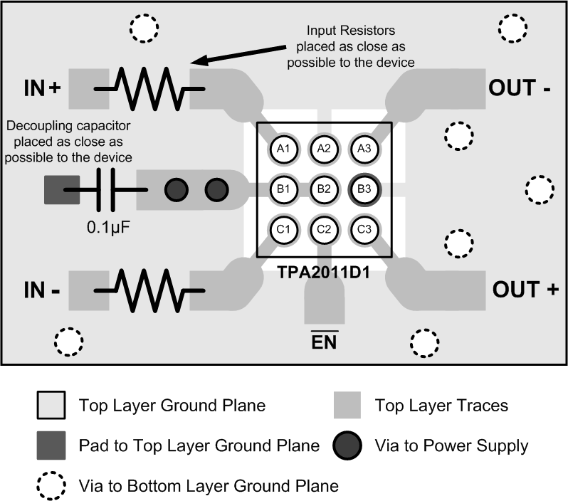
Place all the external components close to the TPA2011D1 device. Placing the decoupling capacitors as close as possible to the device is important for the efficiency of the class-D amplifier. Any resistance or inductance in the trace between the device and the capacitor can cause a loss in efficiency.

An on-pad via is not required to route the middle ball B2 (PVDD) of the TPA2011D1. Just short ball B2 (PVDD) to ball B1 (VDD) and connect both to the supply trace as shown in Figure 37. This simplifies board routing and saves manufacturing cost.
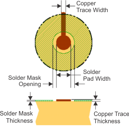
TPA2011D1 land_pat_los524.gif Figure 36. Land Pattern Dimensions

Table 3. Land Pattern Dimensions(1)(2)(3)(4)

SOLDER PAD DEFINITIONS COPPER PAD SOLDER MASK OPENING(5) COPPER THICKNESS STENCIL OPENING(6)(7) STENCIL THICKNESS
Nonsolder mask defined (NSMD) 0.23 mm 0.310 mm 1 oz max
(0.032 mm)
0.275 mm x 0.275 mm Sq.
(rounded corners)
0.1 mm thick
(1) Circuit traces from NSMD defined PWB lands should be 75 μm to 100 μm wide in the exposed area inside the solder mask opening. Wider trace widths reduce device stand off and impact reliability.
(2) Best reliability results are achieved when the PWB laminate glass transition temperature is above the operating the range of the intended application.
(3) Recommend solder paste is Type 3 or Type 4.
(4) For a PWB using a Ni/Au surface finish, the gold thickness should be less 0.5 mm to avoid a reduction in thermal fatigue performance.
(5) Solder mask thickness should be less than 20 μm on top of the copper circuit pattern.
(6) Best solder stencil performance is achieved using laser cut stencils with electro polishing. Use of chemically etched stencils give inferior solder paste volume control.
(7) Trace routing away from DSBGA device should be balanced in X and Y directions to avoid unintentional component movement due to solder wetting forces.

12.2 Layout Example

TPA2011D1 layout_example_slos626.gif Figure 37. TPA2011D1 Layout Example