SLOS438F December 2004 – March 2017 TPA2012D2
PRODUCTION DATA.
- 1 Features
- 2 Applications
- 3 Description
- 4 Revision History
- 5 Device Comparison Table
- 6 Pin Configuration and Functions
- 7 Specifications
- 8 Parameter Measurement Information
- 9 Detailed Description
- 10Application and Implementation
- 11Power Supply Recommendations
- 12Layout
- 13Device and Documentation Support
- 14Mechanical, Packaging, and Orderable Information
Package Options
Mechanical Data (Package|Pins)
Thermal pad, mechanical data (Package|Pins)
- RTJ|20
Orderable Information
9 Detailed Description
9.1 Overview
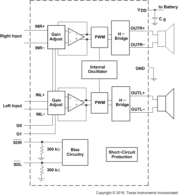
The TPA2012D2 is capable of driving 1.4 W/Ch at 5-V or 720 mW/Ch at 3.6-V into 8 Ω. The TPA2012D2 is also capable of driving a load of 4 Ω.
The TPA2012D2 feature independent shutdown controls for each channel. High PSRR and differential architecture provide increased immunity to noise and RF rectification. The TPA2012D2 provides thermal and short-circuit protection.
9.2 Functional Block Diagram

9.3 Feature Description
9.3.1 Fixed Gain Setting
The TPA2012D2 has 4 selectable fixed gains: 6 dB, 12 dB, 18 dB, and 24 dB. Connect the G0 and G1 pins as shown in Table 1.
Table 1. Gain Setting
| G1 | G0 | GAIN (V/V) |
GAIN (dB) |
INPUT IMPEDANCE (RI, kΩ) |
|---|---|---|---|---|
| 0 | 0 | 2 | 6 | 28.1 |
| 0 | 1 | 4 | 12 | 17.3 |
| 1 | 0 | 8 | 18 | 9.8 |
| 1 | 1 | 16 | 24 | 5.2 |
9.3.2 Short-Circuit Protection
TPA2012D2 goes to low duty cycle mode when a short-circuit event happens. To return to normal duty cycle mode, the device must be reset. The shutdown mode can be set through the SDL and SDR pins, or the device can be turned off and turned on to return to normal duty cycle mode. This feature protects the device without affecting long-term reliability.
9.3.3 Operation With DACs and CODECs
In using Class-D amplifiers with CODECs and DACs, sometimes there is an increase in the output noise floor from the audio amplifier. This occurs when mixing of the output frequencies of the CODEC and DAC mix with the switching frequencies of the audio amplifier input stage. The noise increase can be solved by placing a low-pass filter between the CODEC, DAC, and audio amplifier. This filters off the high frequencies that cause the problem and allow proper performance. The recommended resistor value is 100 Ω and the capacitor value of 47 nF. Figure 35 shows the typical input filter.
 Figure 35. Reducing Out-of-Band DAC Noise With External Input Filter
9.3.4 Filter-Free Operation and Ferrite Bead Filters
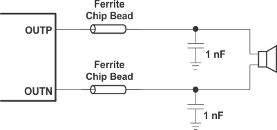
A ferrite bead filter can often be used if the design is failing radiated emissions without an LC filter and the frequency sensitive circuit is greater than 1 MHz. This filter functions well for circuits that just have to pass FCC and CE because FCC and CE only test radiated emissions greater than 30 MHz. When choosing a ferrite bead, choose one with high impedance at high frequencies, and very low impedance at low frequencies. In addition, select a ferrite bead with adequate current rating to prevent distortion of the output signal.
Use an LC output filter if there are low frequency (< 1 MHz) EMI sensitive circuits and/or there are long leads from amplifier to speaker.
Figure 36 shows typical ferrite bead and LC output filters.
 Figure 36. Typical Ferrite Chip Bead Filter (Chip Bead Example: TDK – MPZ1608S221A)
9.4 Device Functional Modes
9.4.1 Shutdown Mode
The TPA2012D2 amplifier can be put in shutdown mode when asserting SDR and SDL pins to a logic LOW. While in shutdown mode, the device output stage is turned off and the current consumption is very low.