SLOS524E June 2008 – May 2016 TPA2016D2
PRODUCTION DATA.
- 1 Features
- 2 Applications
- 3 Description
- 4 Revision History
- 5 Device Comparison Table
- 6 Pin Configuration and Functions
- 7 Specifications
- 8 Parameter Measurement Information
- 9 Detailed Description
- 10Application and Implementation
- 11Power Supply Recommendations
- 12Layout
- 13Device and Documentation Support
- 14Mechanical, Packaging, and Orderable Information
Package Options
Mechanical Data (Package|Pins)
Thermal pad, mechanical data (Package|Pins)
- RTJ|20
Orderable Information
1 Features
- Filter-Free Class-D Architecture
- 1.7 W/Ch Into 8 Ω at 5 V (10% THD+N)
- 750 mW/Ch Into 8 Ω at 3.6 V (10% THD+N)
- 2.8 W/Ch Into 4 Ω at 5 V (10% THD+N)
- 1.5 W/Ch Into 4 Ω at 3.6 V (10% THD+N)
- Power Supply Range: 2.5 V to 5.5 V
- Flexible Operation With or Without I2C
- Programmable DRC and AGC Parameters
- Digital I2C Volume Control
- Selectable Gain from –28 dB to 30 dB in 1-dB Steps (When Compression is Used)
- Selectable Attack, Release, and Hold Times
- 4 Selectable Compression Ratios
- Low Supply Current: 3.5 mA
- Low Shutdown Current: 0.2 μA
- High PSRR: 80 dB
- Fast Start-Up Time: 5 ms
- AGC Enable or Disable Function
- Limiter Enable or Disable Function
- Short-Circuit and Thermal Protection
- Space-Saving Package
- 2.2 mm × 2.2 mm Nano-Free™ DSBGA (YZH)
2 Applications
- Wireless or Cellular Handsets and PDAs
- Portable Navigation Devices
- Portable DVD Players
- Notebook PCs
- Portable Radios
- Portable Games
- Educational Toys
- USB Speakers
3 Description
The TPA2016D2 device is a stereo, filter-free Class-D audio power amplifier with volume control, dynamic range compression (DRC), and automatic gain control (AGC). It is available in a 2.2 mm × 2.2 mm DSBGA package and 20-pin QFN package.
The DRC and AGC function in the TPA2016D2 is programmable through a digital I2C interface. The DRC and AGC function can be configured to automatically prevent distortion of the audio signal and enhance quiet passages that are normally not heard. The DRC and AGC can also be configured to protect the speaker from damage at high power levels and compress the dynamic range of music to fit within the dynamic range of the speaker. The gain can be selected from –28 dB to +30 dB in 1-dB steps.
The TPA2016D2 is capable of driving 1.7 W/Ch at 5 V or 750 mW/Ch at 3.6 V into 8-Ω load or 2.8 W/Ch at 5 V or 1.5 W/Ch at 3.6 V into 4-Ω load. The device features independent software shutdown controls for each channel and also provides thermal and short-circuit protection.
In addition to these features, a fast start-up time and small package size make the TPA2016D2 an ideal choice for cellular handsets, PDAs, and other portable applications.
Device Information(1)
| PART NUMBER | PACKAGE | BODY SIZE (NOM) |
|---|---|---|
| TPA2016D2 | DSBGA (16) | 2.20 mm × 2.20 mm |
| QFN (20) | 4.00 mm × 4.00 mm |
- For all available packages, see the orderable addendum at the end of the data sheet.
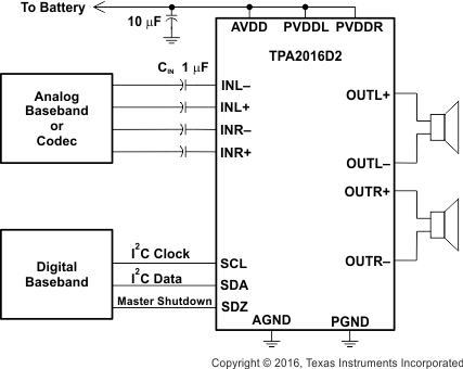
Simplified Application Diagram

4 Revision History
Changes from D Revision (August 2009) to E Revision
- Added ESD Ratings table, Feature Description section, Device Functional Modes, Application and Implementation section, Power Supply Recommendations section, Layout section, Device and Documentation Support section, and Mechanical, Packaging, and Orderable Information section.Go
Changes from C Revision (October 2008) to D Revision
- Added Feature: 2.8 W/Ch Into 4 Ω at 5 V (10% THD+N)Go
- Added Feature: 1.5 W/Ch Into 4 Ω at 3.6 V (10% THD+N)Go
- Added the RTJ (QFN) pin out packageGo
- Changed the RTJ Package Options to the Available Options TableGo
- Changed ISWS Softwre shutdown 3.6V From: Max 60 to: 70 µAGo
- Changed ISWS Softwre shutdown 5.5V From: Max 100 to 110 µAGo
- Changed Output offset TYP From 0 mV To: 2 mVGo
- Added the RTJ (QFN) package to the Dissipation Ratings Table.Go
- Deleted Table of Graphs from the Typical Characteristics.Go
- Added 4Ω Efficiency GraphGo
- Added 4Ω Total Power Dissipation GraphGo
- Added 4Ω Total Supply Current GraphGo
- Added QFN Output Power GraphGo
- Added text notes 4 and 5 to the Test Setup for Graphs.Go
Changes from B Revision (June 2008) to C Revision
- Changed RLOADfrom 6.4 Ω to 3.2ΩGo
Changes from A Revision (June 2008) to B Revision
- Changed Feature High PSRR From: 75 dB at 217 Hz To: 80 dBGo
- Added 00 to Default columnGo
- Added 00 to Default columnGo
- Added 00 to Default columnGo
Changes from * Revision (June 2008) to A Revision
- Changed From: 1.4 W/Ch Into 8 Ω at 5 V (10% THD+N) To: 1.7 W/Ch Into 8 Ω at 5 V (10% THD+N)Go