SLOS717B August 2011 – December 2014 TPA2025D1
PRODUCTION DATA.
- 1 Features
- 2 Applications
- 3 Description
- 4 Revision History
- 5 Device Comparison Table
- 6 Pin Configuration and Functions
- 7 Specifications
- 8 Parameter Measurement Information
- 9 Detailed Description
- 10Application and Implementation
- 11Power Supply Recommendations
- 12Layout
- 13Device and Documentation Support
- 14Mechanical, Packaging, and Orderable Information
Package Options
Mechanical Data (Package|Pins)
- YZG|12
Thermal pad, mechanical data (Package|Pins)
Orderable Information
6 Pin Configuration and Functions
12-PIN
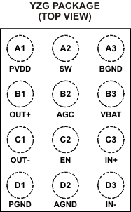
Pin Functions
| PIN | INPUT/ OUTPUT/ POWER (I/O/P) | DESCRIPTION | |
|---|---|---|---|
| NAME | WCSP | ||
| PVDD | A1 | O | Boost converter output and Class-D power stage supply voltage. |
| SW | A2 | I | Boost converter switch input; connect boost inductor between VBAT and SW. |
| BGND | A3 | P | Boost converter power ground. |
| OUT+ | B1 | O | Positive audio output. |
| AGC | B2 | I | AGC inflection point select. Connect to VDD, GND or Float. Voltage at AGC pin is only read at device power-up. A power cycle is required to change inflection points. |
| VBAT | B3 | P | Supply voltage. |
| OUT– | C1 | O | Negative audio output. |
| EN | C2 | I | Device enable; set to logic high to enable. |
| IN+ | C3 | I | Positive audio input. |
| PGND | D1 | P | Class-D power ground. |
| AGND | D2 | P | Analog ground. |
| IN– | D3 | I | Negative audio input. |