SLOS733B January 2012 – April 2016 TPA2080D1
PRODUCTION DATA.
- 1 Features
- 2 Applications
- 3 Description
- 4 Revision History
- 5 Device Comparison Table
- 6 Pin Configuration and Functions
- 7 Specifications
- 8 Parameter Measurement Information
- 9 Detailed Description
- 10Application and Implementation
- 11Power Supply Recommendations
- 12Layout
- 13Device and Documentation Support
- 14Mechanical, Packaging, and Orderable Information
Package Options
Mechanical Data (Package|Pins)
- YZG|12
Thermal pad, mechanical data (Package|Pins)
Orderable Information
10 Application and Implementation
NOTE
Information in the following applications sections is not part of the TI component specification, and TI does not warrant its accuracy or completeness. TI’s customers are responsible for determining suitability of components for their purposes. Customers should validate and test their design implementation to confirm system functionality.
10.1 Application Information
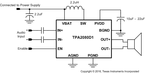
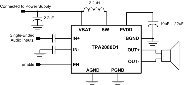
These typical connection diagrams highlight the required external components and system level connections for proper operation of the device. Each of these configurations can be realized using the Evaluation Modules (EVMs) for the device. These flexible modules allow full evaluation of the device in the most common modes of operation. Any design variation can be supported by TI through schematic and layout reviews. Visit e2e.ti.com for design assistance and join the audio amplifier discussion forum for additional information.
10.2 Typical Application
10.2.1 TPA2080D1 With Differential Input Signal
 Figure 23. Typical Application Schematic With Differential Input Signals
10.2.1.1 Design Requirements
For this design example, use the parameters listed in Table 2.
Table 2. Design Parameters
| DESIGN PARAMETER | EXAMPLE VALUE |
|---|---|
| Power supply | 3.6 V |
| Enable inputs | High > 1.3 V |
| Low < 0.6 V | |
| Speaker | 8 Ω |
10.2.1.2 Detailed Design Procedure
10.2.1.2.1 Surface Mount Inductor
Working inductance decreases as inductor current increases. if the drop in working inductance is severe enough, it may cause the boost converter to become unstable, or cause the TPA2080D1 to reach its current limit at a lower output power than expected. Inductor vendors specify currents at while inductor values decrease by a specific percentage. This can vary from 10% to 35%. Inductance is also affected by DC current and temperature.
10.2.1.2.2 Inductor Selection
Inductor current rating is determined by the requirements of the load. The inductance is determined by two factors: the minimum value required for stability and the maximum ripple current permitted in the application. Use Equation 1 to determine the required current rating. Equation 1 shows the approximate relationship between the average inductor current, IL, to the load current, load voltage, and input voltage (IPVDD, PVDD, and VBAT, respectively). Insert IPVDD, PVDD, and VBAT into Equation 1 and solve for IL. The inductor must maintain at least 90% of its initial inductance value at this current.

Ripple current, ΔIL, is peak-to-peak variation in inductor current. Smaller ripple current reduces core losses in the inductor and reduces the potential for EMI. Use Equation 2 to determine the value of the inductor, L. Equation 2 shows the relationship between inductance L, VBAT, PVDD, the switching frequency, fBOOST, and ΔIL. Insert the maximum acceptable ripple current into Equation 2 and solve for L.

ΔIL is inversely proportional to L. Minimize ΔIL as much as is necessary for a specific application. Increase the inductance to reduce the ripple current. Do not use greater than 4.7 μH, as this prevents the boost converter from responding to fast output current changes properly. If using above 3.3 µH, then use at least 10-µF capacitance on PVDD to ensure boost converter stability.
The typical inductor value range for the TPA2080D1 is 2.2 μH to 3.3 µH. Select an inductor with less than 0.5-Ω DC resistance, DCR. Higher DCR reduces total efficiency due to an increase in voltage drop across the inductor.
Table 3. Sample Inductors
| L (µH) |
SUPPLIER | COMPONENT CODE | SIZE (LxWxH mm) |
DCR TYP (mΩ) |
ISAT MAX (A) |
C RANGE |
|---|---|---|---|---|---|---|
| 2.2 | Chilisin Electronics Corp. | CLCN252012T-2R2M-N | 2.5 x 2 x 1.2 | 105 | 1.2 | 10 to 22 µF, 16 V 10 to 22 µF, 10 V |
| 2.2 | Toko | 1239AS-H-2R2N=P2 | 2.5 x 2 x 1.2 | 96 | 2.3 | |
| 2.2 | Coilcraft | XFL4020-222MEC | 4 x 4 x 2.15 | 22 | 3.5 | |
| 3.3 | Toko | 1239AS-H-3R3N=P2 | 2.5 x 2 x 1.2 | 160 | 2 | 10 to 22 µF, 10 V |
| 3.3 | Coilcraft | XFL4020-332MEC | 4 x 4 x 2.15 | 35 | 2.8 |
10.2.1.2.3 Surface Mount Capacitors
Temperature and applied DC voltage influence the actual capacitance of high-K materials. Table 4 shows the relationship between the different types of high-K materials and their associated tolerances, temperature coefficients, and temperature ranges. Notice that a capacitor made with X5R material can lose up to 15% of its capacitance within its working temperature range.
In an application, the working capacitance of components made with high-K materials is generally much lower than nominal capacitance. A worst-case result with a typical X5R material might be –10% tolerance, –15% temperature effect, and –45% DC voltage effect at 50% of the rated voltage. This particular case would result in a working capacitance of 42% (0.9 × 0.85 × 0.55) of the nominal value.
Select high-K ceramic capacitors according to the following rules:
- Use capacitors made of materials with temperature coefficients of X5R, X7R, or better.
- Use capacitors with DC voltage ratings of at least twice the application voltage. Use minimum 10-V capacitors for the TPA2080D1.
- Choose a capacitance value at least twice the nominal value calculated for the application. Multiply the nominal value by a factor of 2 for safety. If a 10-μF capacitor is required, use 20 µF.
The preceding rules and recommendations apply to capacitors used in connection with the TPA2080D1. The TPA2080D1 cannot meet its performance specifications if the rules and recommendations are not followed.
Table 4. Typical Tolerance and Temperature Coefficient of Capacitance by Material
| MATERIAL | COG / NPO | X7R | X5R |
|---|---|---|---|
| Typical tolerance | ±5% | ±10% | 80% or –20% |
| Temperature | ±30 ppm | ±15% | 22% or –82% |
| Temperature range, °C | –55°C to 125°C | –55°C to 125°C | –30°C to 85°C |
10.2.1.2.4 Boost Converter Capacitor Selection
The value of the boost capacitor is determined by the minimum value of working capacitance required for stability and the maximum voltage ripple allowed on PVDD in the application. Working capacitance refers to the available capacitance after derating the capacitor value for DC bias, temperature, and aging. Do not use any component with a working capacitance less than 6.8 µF. This corresponds to a 10-μF, 16-V capacitor or a 10-μF, 10-V capacitor.
Do not use above 22-μF capacitance as it will reduce the boost converter response time to large output current transients.
Equation 3 shows the relationship between the boost capacitance, C, to load current, load voltage, ripple voltage, input voltage, and switching frequency (IPVDD, PVDD, ΔV, VBAT, and fBOOST respectively).
Insert the maximum allowed ripple voltage into Equation 3 and solve for C. The 1.5 multiplier accounts for capacitance loss due to applied DC voltage and temperature for X5R and X7R ceramic capacitors.

10.2.1.2.5 Decoupling Capacitors
The TPA2080D1 is a high-performance Class-D audio amplifier that requires adequate power supply decoupling. Adequate power supply decoupling to ensures that the efficiency is high and total harmonic distortion (THD) is low.
Place a low equivalent-series-resistance (ESR) ceramic capacitor, typically 0.1 µF, within 2 mm of the VBAT ball. Use X5R and X7R ceramic capacitors. This choice of capacitor and placement helps with higher frequency transients, spikes, or digital hash on the line. Additionally, placing this decoupling capacitor close to the TPA2080D1 is important, as any parasitic resistance or inductance between the device and the capacitor causes efficiency loss. In addition to the 0.1-μF ceramic capacitor, place a 2.2-µF to 10-µF capacitor on the VBAT supply trace. This larger capacitor acts as a charge reservoir, providing energy faster than the board supply, thus helping to prevent any droop in the supply voltage.
10.2.1.2.6 Input Capacitors
Input audio DC decoupling capacitors are recommended. The input capacitors and TPA2080D1 input impedance form a high-pass filter with the corner frequency, fC, determined in Equation 4.
Any mismatch in capacitance between the two inputs will cause a mismatch in the corner frequencies. Severe mismatch may also cause turnon pop noise. Choose capacitors with a tolerance of ±10% or better. Use X5R and X7R ceramic capacitors.

The value of the input capacitor is important to consider as it directly affects the bass (low frequency) performance of the circuit. Speakers in wireless phones cannot usually respond well to low frequencies, so the corner frequency can be set to block low frequencies in this application. Not using input capacitors can increase output offset.
10.2.1.2.7 Boost Converter Component Section
The critical external components are summarized in Table 5.
Table 5. Recommended Values
| PARAMETER | TEST CONDITIONS | MIN | TYP | MAX | UNIT |
|---|---|---|---|---|---|
| Boost converter inductor | At 30% rated DC bias current of the inductor | 1.5 | 2.2 | 4.7 | µH |
| Input capacitor | 1 | 10 | µF | ||
| Boost converter output capacitor | Working capacitance biased at boost output voltage, if 4.7-µH inductor is chosen, then minimum capacitance is 10 µF | 4.7 | 22 | µF |
10.2.2 TPA2080D1 With Single-Ended Signals.
 Figure 24. Typical Application Schematic With Single-Ended Input Signal
10.2.2.1 Design Requirements
For this design example, use the parameters listed in Table 2.
10.2.2.2 Detailed Design Procedure
For the design procedure see Detailed Design Procedure.
10.2.2.3 Application Curves
For application curves, see the figures listed in Table 6.