SLVSBC5D March 2012 – October 2015 TPD13S523
PRODUCTION DATA.
- 1 Features
- 2 Applications
- 3 Description
- 4 Revision History
- 5 Pin Configuration and Functions
- 6 Specifications
-
7 Detailed Description
- 7.1 Overview
- 7.2 Functional Block Diagram
- 7.3
Feature Description
- 7.3.1 IEC 61000-4-2 Protection
- 7.3.2 Single-Chip ESD Solution
- 7.3.3 On-Chip 5-V Load Switch
- 7.3.4 Supports UTILITY Line Protection
- 7.3.5 < 0.05-pF Differential Capacitance Between TMDS Pairs
- 7.3.6 Industry Standard Package and Space-Saving Package
- 7.3.7 Supports Data Rates in Excess of 3.4 Gbps
- 7.3.8 RDYN = 0.5 Ω
- 7.3.9 Commercial Temperature Range
- 7.4 Device Functional Modes
- 8 Application and Implementation
- 9 Power Supply Recommendations
- 10Layout
- 11Device and Documentation Support
- 12Mechanical, Packaging, and Orderable Information
Package Options
Mechanical Data (Package|Pins)
Thermal pad, mechanical data (Package|Pins)
Orderable Information
8 Application and Implementation
NOTE
Information in the following applications sections is not part of the TI component specification, and TI does not warrant its accuracy or completeness. TI’s customers are responsible for determining suitability of components for their purposes. Customers should validate and test their design implementation to confirm system functionality.
8.1 Application Information
The TPD13S523 provides IEC 61000-4-2 Level 4 Contact ESD protection for an HDMI 1.4 transmitter port. An integrated current limit switch ensures compliance with the HDMI 5-V power supply requirements. This section presents a simplified discussion of the design process for this protection device.
8.2 Typical Application
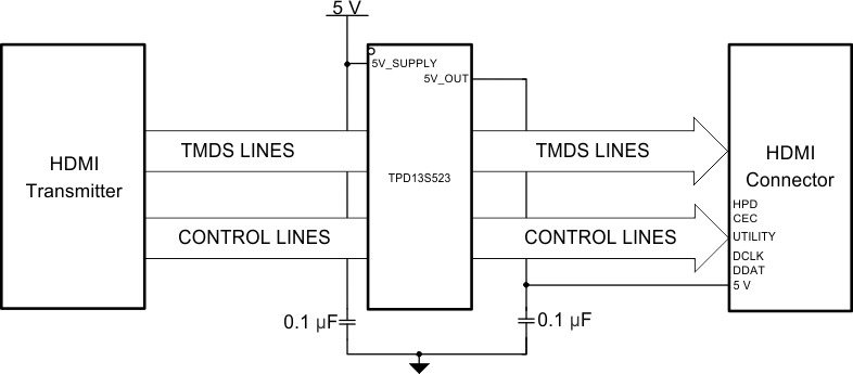
A typical application schematic for an HDMI 1.4 transmitter port protected by the TPD13S523 is shown in Figure 11. The eight TMDS lines and five control lines are connected to their respective pins for ESD protection. The 5-V power path is connected through the 55-mA current limit switch.
 Figure 11. TPD13S523 Configured With an HDMI 1.4 Transmitter Port
8.2.1 Design Requirements
For this design example, use the parameters listed in Table 1 as input parameters.
Table 1. Design Parameters
| PARAMETER | EXAMPLE VALUE |
|---|---|
| Voltage on 5V_SUPPLY | 4.8 V - 5.3 V |
| HDMI Data Rate | 3.4 Gbps |
8.2.2 Detailed Design Procedure
To begin the design process, the designer must know the following parameters:
- 5V_SUPPLY voltage range
- Maximum HDMI data rate
8.2.2.1 5V_SUPPLY Voltage Range
The TPD13S523 is capable of operating the 5V_SUPPLY up to 5.5 V, with recommended voltage from 4.5 V to 5.5 V. In this example, the supply range is 4.8 V to 5.3 V, which satisfies this requirement.
8.2.2.2 Maximum HDMI Data Rate
The TPD13S523 is capable of operating at HDMI data rates in excess of 3.4 Gbps, compliant to the HDMI 1.4 maximum data rate. In this example, the maximum HDMI 1.4 data rate of 3.4 Gbps has been chosen.
8.2.3 Application Curves
 Figure 12. Eye Diagram Using EVM Without TPD13S523 for the TMDS Lines
at 1080p, 340-MHz Pixel Clock, 3.4 Gbps
 Figure 13. Eye Diagram Using EVM With TPD13S523 for the TMDS Lines
at 1080p, 340-MHz Pixel Clock, 3.4 Gbps