SLVSBC5D March 2012 – October 2015 TPD13S523
PRODUCTION DATA.
- 1 Features
- 2 Applications
- 3 Description
- 4 Revision History
- 5 Pin Configuration and Functions
- 6 Specifications
-
7 Detailed Description
- 7.1 Overview
- 7.2 Functional Block Diagram
- 7.3
Feature Description
- 7.3.1 IEC 61000-4-2 Protection
- 7.3.2 Single-Chip ESD Solution
- 7.3.3 On-Chip 5-V Load Switch
- 7.3.4 Supports UTILITY Line Protection
- 7.3.5 < 0.05-pF Differential Capacitance Between TMDS Pairs
- 7.3.6 Industry Standard Package and Space-Saving Package
- 7.3.7 Supports Data Rates in Excess of 3.4 Gbps
- 7.3.8 RDYN = 0.5 Ω
- 7.3.9 Commercial Temperature Range
- 7.4 Device Functional Modes
- 8 Application and Implementation
- 9 Power Supply Recommendations
- 10Layout
- 11Device and Documentation Support
- 12Mechanical, Packaging, and Orderable Information
Package Options
Mechanical Data (Package|Pins)
Thermal pad, mechanical data (Package|Pins)
Orderable Information
7 Detailed Description
7.1 Overview
The TPD13S523 device is a single-chip ESD solution for the HDMI transmitter port. By providing system-level ESD protection for a full HDMI port, the TPD13S523 can protect the core IC from ESD strikes and absorb the associated energy.
While providing the ESD protection, the TPD13S523 adds little-to-no signal distortion to the high-speed differential signals. In addition, the monolithic integrated circuit technology ensures that there is excellent matching between the two-signal pair of the differential line.
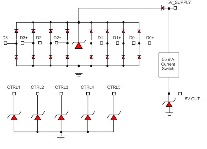
The TPD13S523 also provides an on-chip regulator with current output ratings of 55 mA at pin 38. This current enables HDMI receiver detection even when the receiver device is powered off.
7.2 Functional Block Diagram
 Figure 10. Electrical Equivalent Circuit Diagrams
7.3 Feature Description
7.3.1 IEC 61000-4-2 Protection
The connector-facing I/O pins can withstand ESD events up to ±12-kV contact and ±14-kV air. An ESD clamp diverts the current to ground.
7.3.2 Single-Chip ESD Solution
The TPD13S523 provides a complete ESD protection scheme for an HDMI 1.4 compliant port. No additional components are required for ESD protection and current-limiting besides this device.
7.3.3 On-Chip 5-V Load Switch
The TPD13S523 provides an on-chip regulator with a current output rating of 55-mA. This regulator also prevents reverse current flow from occurring, in compliance with the HDMI 5-V supply specification.
7.3.4 Supports UTILITY Line Protection
This device provides protection for all control lines in HDMI, including the UTILITY pin.
7.3.5 < 0.05-pF Differential Capacitance Between TMDS Pairs
The TPD13S523 has a very low capacitance variation (< 0.05 pF) between different TMDS ESD clamps. This provides excellent matching and does not degrade differential signal quality.
7.3.6 Industry Standard Package and Space-Saving Package
The TPD13S523 is offered in 2 different packages. A 16-pin industry standard TSSOP package is provided for ease of routing and easy layout. A 16-pin UQFN (RSV) is provided where small size is needed in the application.
7.3.7 Supports Data Rates in Excess of 3.4 Gbps
The TMDS ESD clamps have a very low capacitance that is capable of supporting HDMI data rates exceeding 3.4 Gbps.
7.3.8 RDYN = 0.5 Ω
The TMDS ESD clamps have a very low RDYN of 0.5Ω (typ) which provides excellent ESD protection clamping characteristics for the upstream core transmitter.
7.3.9 Commercial Temperature Range
The TPD13S523 is rated to operate from -40°C to 85°C.
7.4 Device Functional Modes
TPD13S523 is active with the conditions in the Recommended Operating Conditions met. Each connector side pin has an ESD clamp that triggers when voltages are greater than VBR or less than the lower diode's Vf. During ESD events, voltages as high as ±12-kV contact ESD can be directed to ground through the internal diode network. Once the voltages on the protected line fall below these trigger levels (usually within 10's of nano-seconds), these pins revert to a nonconductive state.