SLLS683F JULY 2006 – October 2015 TPD3E001
PRODUCTION DATA.
- 1 Features
- 2 Applications
- 3 Description
- 4 Revision History
- 5 Pin Configuration and Functions
- 6 Specifications
- 7 Detailed Description
- 8 Application and Implementation
- 9 Power Supply Recommendations
- 10Layout
- 11Device and Documentation Support
- 12Mechanical, Packaging, and Orderable Information
Package Options
Refer to the PDF data sheet for device specific package drawings
Mechanical Data (Package|Pins)
- DRS|6
- DRL|5
- DRY|6
Thermal pad, mechanical data (Package|Pins)
Orderable Information
8 Application and Implementation
NOTE
Information in the following applications sections is not part of the TI component specification, and TI does not warrant its accuracy or completeness. TI’s customers are responsible for determining suitability of components for their purposes. Customers should validate and test their design implementation to confirm system functionality.
8.1 Application Information
TPD3E001 is a diode array type Transient Voltage Suppressor (TVS) which is typically used to provide a path to ground for dissipating ESD events on hi-speed signal lines between a human interface connector and a system. As the current from ESD passes through the TVS, only a small voltage drop is present across the diode. This is the voltage presented to the protected IC. The low RDYN of the triggered TVS holds this voltage, VCLAMP, to a tolerable level to the protected IC.
8.2 Typical Application
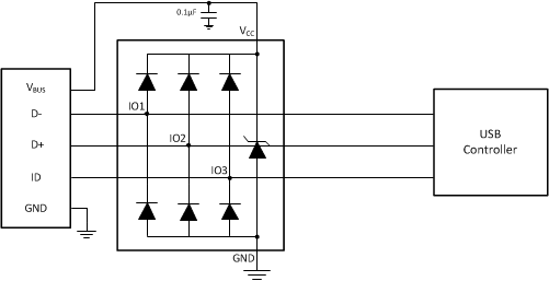
 Figure 3. Typical Application Schematic
8.2.1 Design Requirements
For this design example, a single TPD3E001 is used to protect all the pins of a USB2.0 micro-AB connector. The micro-AB connector has an extra pin, the ID pin, which is used by the device to determine whether it is to perform the "A" role or the "B' role. This functionality the ID offers is part of the USB On-the-Go (OTG) Standard. The TPD3E001 offers 3-channels of IEC Level ESD protection to provide complete protection for the USB micro-AB style connector, plus VCC (VBUS, D+, D-, ID).
Given the USB application, the following parameters are known.
Table 1. Design Parameters
| DESIGN PARAMETER | EXAMPLE VALUE |
|---|---|
| Signal range on IO1, IO2 | 0 V to 3.6 V |
| State of IO3 (ID) | GND or Floating |
| Signal voltage range on VCC | 0 V to 5.25 V |
| Operating Frequency | 240 MHz |
8.2.2 Detailed Design Procedure
When placed near the USB connectors, the TPD3E001 ESD solution offers little or no signal distortion during normal operation due to low IO capacitance and ultra-low leakage current specifications. The TPD3E001 ensures that the core circuitry is protected and the system is functioning properly in the event of an ESD strike. For proper operation, the following layout/ design guidelines should be followed:
- Place the TPD3E001 solution close to the connectors. This allows the TPD3E001 to take away the energy associated with ESD strike before it reaches the internal circuitry of the system board.
- Place a 0.1-μF capacitor very close to the VCC pin. This limits any momentary voltage surge at the IO pin during the ESD strike event.
- Ensure that there is enough metallization for the VCC and GND loop. During normal operation, the TPD3E001 consumes approximately 1 nA (typ.) supply current through the VCC and GND loop. But during the ESD event, VCC and GND may see 15 A to 30 A of current, depending on the ESD level. Sufficient current path enables safe discharge of all the energy associated with the ESD strike.
- Leave the unused IO pins floating. In this example of protecting a micro-AB type USB port, none of the IO pins will be left unused.
- The VCC pin can be connected in two different ways:
- If the VCC pin is connected to the system power supply, the TPD3E001 works as a transient suppressor for any signal swing above VCC + VF. A 0.1-μF capacitor on the device VCC pin is recommended for ESD bypass.
- If the VCC pin is not connected to the system power supply, the TPD3E001 can tolerate higher signal swing in the range up to 10 V. Please note that a 0.1-μF capacitor is still recommended at the VCC pin for ESD bypass.
8.2.3 Application Curve
Figure 4 is a capture of the voltage clamping waveform of TPD3E001 on IO1 during a +8kV Contact IEC61000-4-2 ESD strike.
 Figure 4. TPD3E001 +8kV Contact IEC61000-4-2 Voltage Clamping Waveform