SLUSDH1B may   2020  – april 2023 TPD3S713-Q1 , TPD3S713A-Q1

PRODUCTION DATA  

  1. Features
  2. Applications
  3. Description
  4. Revision History
  5. Pin Configuration and Functions
  6. Specifications
    1. 6.1 Absolute Maximum Ratings
    2. 6.2 ESD Ratings
    3. 6.3 Recommended Operating Conditions
    4. 6.4 Thermal Information
    5. 6.5 Electrical Characteristics
    6. 6.6 Switching Characteristics
    7. 6.7 Typical Characteristics
  7. Parameter Measurement Information
  8. Detailed Description
    1. 8.1 Overview
    2. 8.2 Functional Block Diagram
    3. 8.3 Feature Description
      1. 8.3.1 FAULT Response
      2. 8.3.2 Cable Compensation
        1. 8.3.2.1 Design Procedure
      3. 8.3.3 DP and DM Protection
      4. 8.3.4 VBUS OVP Protection
      5. 8.3.5 Output and DP or DM Discharge
      6. 8.3.6 Overcurrent Protection
      7. 8.3.7 Undervoltage Lockout
      8. 8.3.8 Thermal Sensing
      9. 8.3.9 Current-Limit Setting
    4. 8.4 Device Functional Modes
      1. 8.4.1 Device Truth Table (TT)
      2. 8.4.2 Client Mode
      3. 8.4.3 High-Bandwidth Data-Line Switch
  9. Application and Implementation
    1. 9.1 Application Information
    2. 9.2 Typical Application
      1. 9.2.1 Design Requirements
      2. 9.2.2 Detailed Design Procedure
        1. 9.2.2.1 Input Capacitance
        2. 9.2.2.2 Output Capacitance
        3. 9.2.2.3 BIAS Capacitance
        4. 9.2.2.4 Output and BIAS TVS
      3. 9.2.3 Application Curves
    3. 9.3 Power Supply Recommendations
    4. 9.4 Layout
      1. 9.4.1 Layout Guidelines
      2. 9.4.2 Layout Example
  10. 10Device and Documentation Support
    1. 10.1 Documentation Support
      1. 10.1.1 Related Documentation
    2. 10.2 Receiving Notification of Documentation Updates
    3. 10.3 Support Resources
    4. 10.4 Trademarks
    5. 10.5 Electrostatic Discharge Caution
    6. 10.6 Glossary
  11. 11Mechanical, Packaging, and Orderable Information

Package Options

Refer to the PDF data sheet for device specific package drawings

Mechanical Data (Package|Pins)
  • RVC|20
Thermal pad, mechanical data (Package|Pins)
Orderable Information

Typical Characteristics

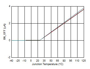
TA = 25°C, V(IN) = 5 V, V(EN) = V(IN), V(ILIM_SEL) = V(INT1) = V(IN), V(INT2) = GND, FAULT connect to V(IN) via a 10-kΩ pullup resistor (unless stated otherwise)
GUID-8FF6D923-604E-42C7-8C9A-50F98F4A730D-low.gif
V(IN) = 5 V
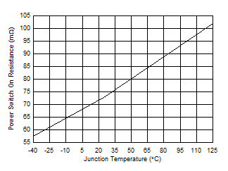
Figure 6-1 Power Switch On-Resistance vs Temperature
GUID-9D4B7466-2CAD-4874-B206-757A8F73F9EA-low.gif
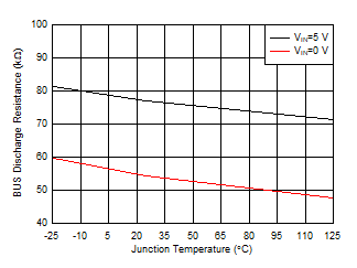
Figure 6-3 BUS Discharge Resistance (OVP) vs Temperature
GUID-EB47CCA1-8AC2-4C2A-B3C3-6C08016873C1-low.gif
V(IN) = 5 V
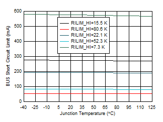
Figure 6-5 VBUS Short-Circuit Current Limit vs Temperature
GUID-9DEB3540-97A7-41BC-8C86-61278FA23C88-low.gif
ILIM_SEL = High
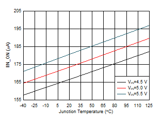
Figure 6-7 Enabled IN Supply Current vs Temperature
GUID-72B023B0-9FCC-494C-8045-0E840F3E2EBD-low.gif
V(IN) = 5 V
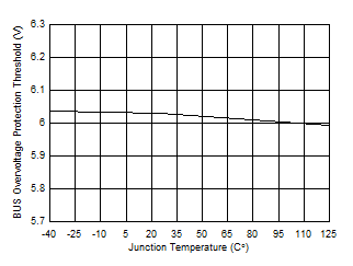
Figure 6-9 BUS Overvoltage Protection Threshold vs Temperature
GUID-F5793765-7564-4BB9-9E68-58A03F5510AA-low.gif
VIN = 5.5 V IBUS = 0.5 A
Figure 6-11 I(CS) vs V(CS) Voltage
GUID-E1C45578-8ADD-4185-AF47-EE8BD898FE9F-low.gif
VIN = 4.5 VIBUS = 0.5 A
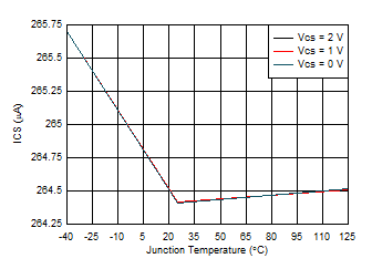
Figure 6-13 I(IMON) vs V(CS) Voltage
GUID-03DCA9A9-7F8A-4124-8B33-8D9979500611-low.gif
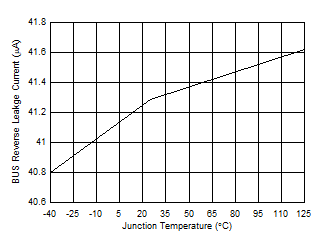
V(OUT) = 5 VMeasure I(BUS)
Figure 6-2 Reverse Leakage Current vs Temperature
GUID-A60D49E9-96FC-4364-BDC3-51EE3B9B2E63-low.gif
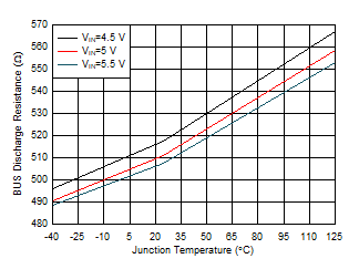
Figure 6-4 BUS Discharge Resistance (Mode Change) vs Temperature
GUID-AB3E7693-FE54-4BA2-8B71-BF77BC002C09-low.gif
ILIM_SEL = High
Figure 6-6 Disabled IN Supply Current vs Temperature
GUID-FAF5CD35-0C14-4852-A024-5C19AB187C12-low.gif
V(IN) = 5 V
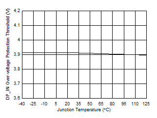
Figure 6-8 DP_IN Overvoltage Protection Threshold vs Temperature
GUID-E80E530E-9540-4727-8D48-D9FE635CD659-low.gif
IBUS = 0.5 A V(CS) = 2.5 V
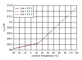
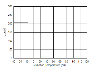
Figure 6-10 I(CS) vs Temperature
GUID-C8602FE7-4A04-4B17-8828-E5910AD800CC-low.gif
IBUS = 0.5 A V(IMON) = 2.5 V
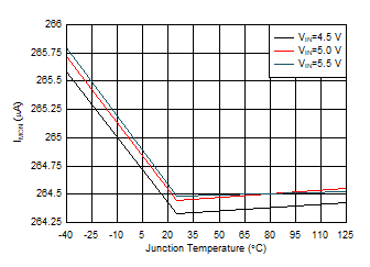
Figure 6-12 I(IMON) vs Temperature
GUID-2A918550-4BD9-4524-9BFD-AF8E717DA868-low.png
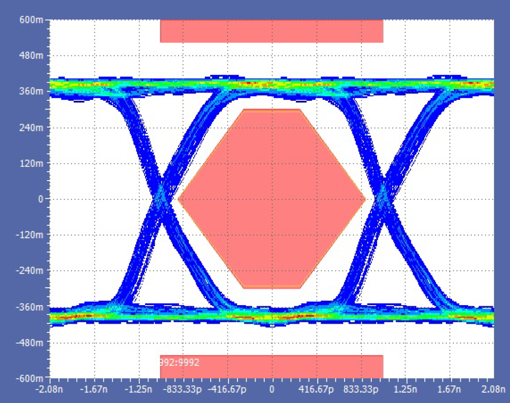
Measured on EVM with 10-cm cable
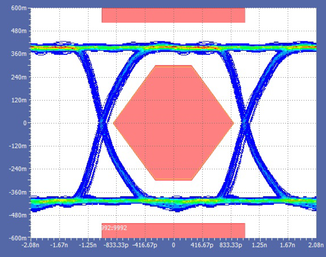
Figure 6-14 Bypassing the TPD3S713-Q1 Data Switch
GUID-368F6AB8-5676-4282-9A9B-5E43E9D93E66-low.png
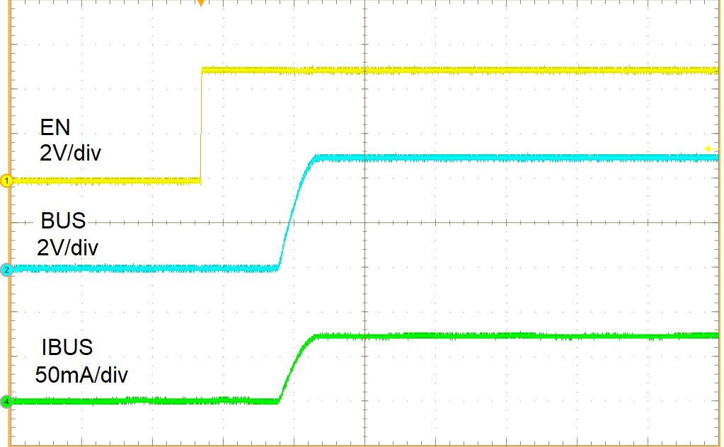
R(LOAD) = 68 ΩC(LOAD) = 10 µFt = 5 ms/div
Figure 6-16 Turn-on Response
GUID-43A2FA37-B20B-47F9-AC97-6FDA5A87F0F6-low.png
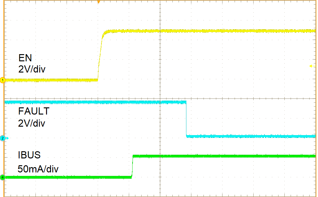
R(ILIM_LO) = 80.6 kΩt = 5 ms/div
Figure 6-18 Enable Into Short
GUID-8CD6D2DB-CB29-4FEB-A9C9-4F7C4A14BAA9-low.png
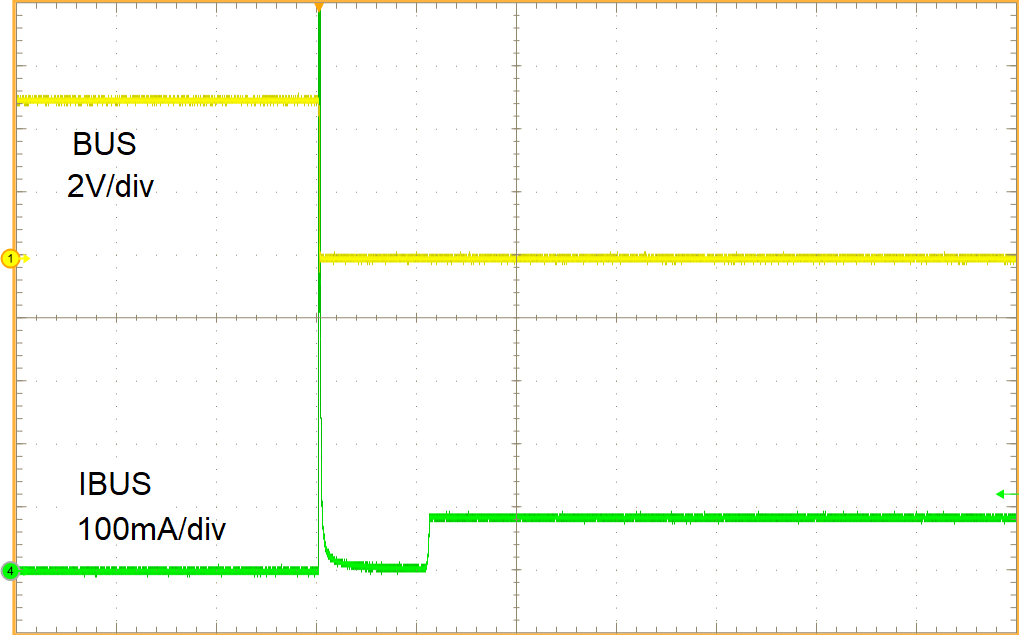
R(ILIM_HI) = 52.3 kΩR(short) = 50 mΩt = 5 ms/div
Figure 6-20 Hot Short
GUID-A73773A5-1156-4388-8685-34D70DF9DB54-low.png
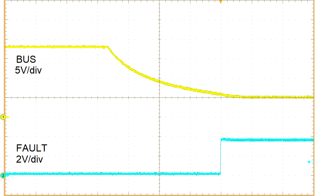
t = 20 ms/div
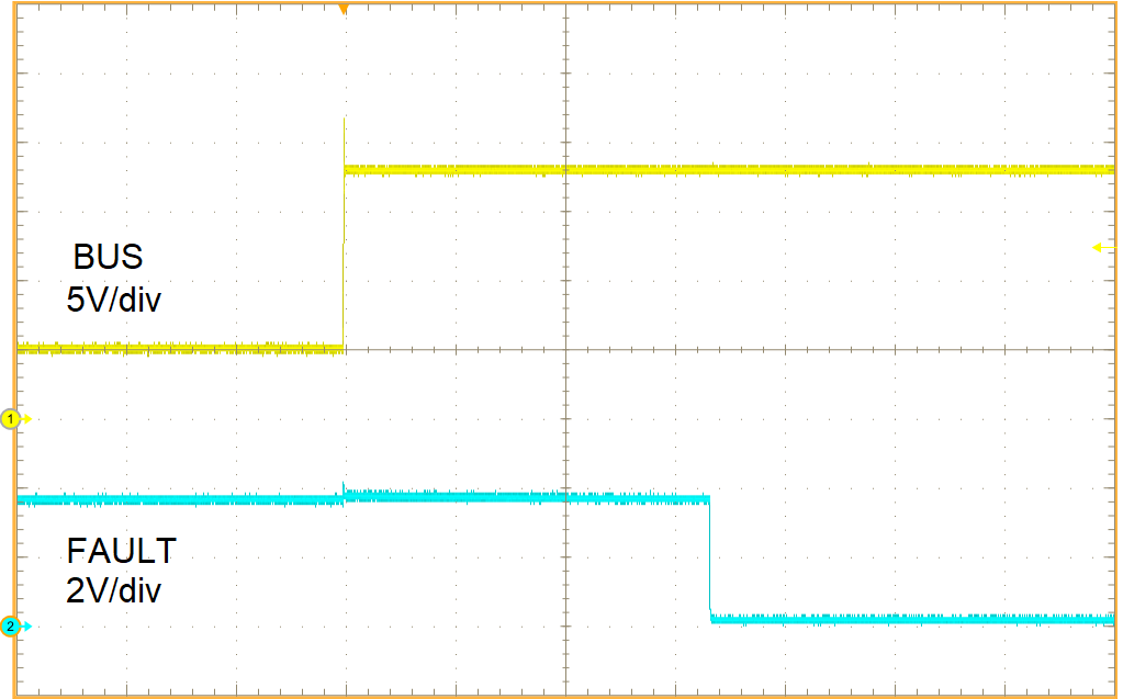
Figure 6-22 VBUS Short-to-Battery Recovery
GUID-2E159415-4E50-4C21-883F-3F6D582A6D8F-low.png
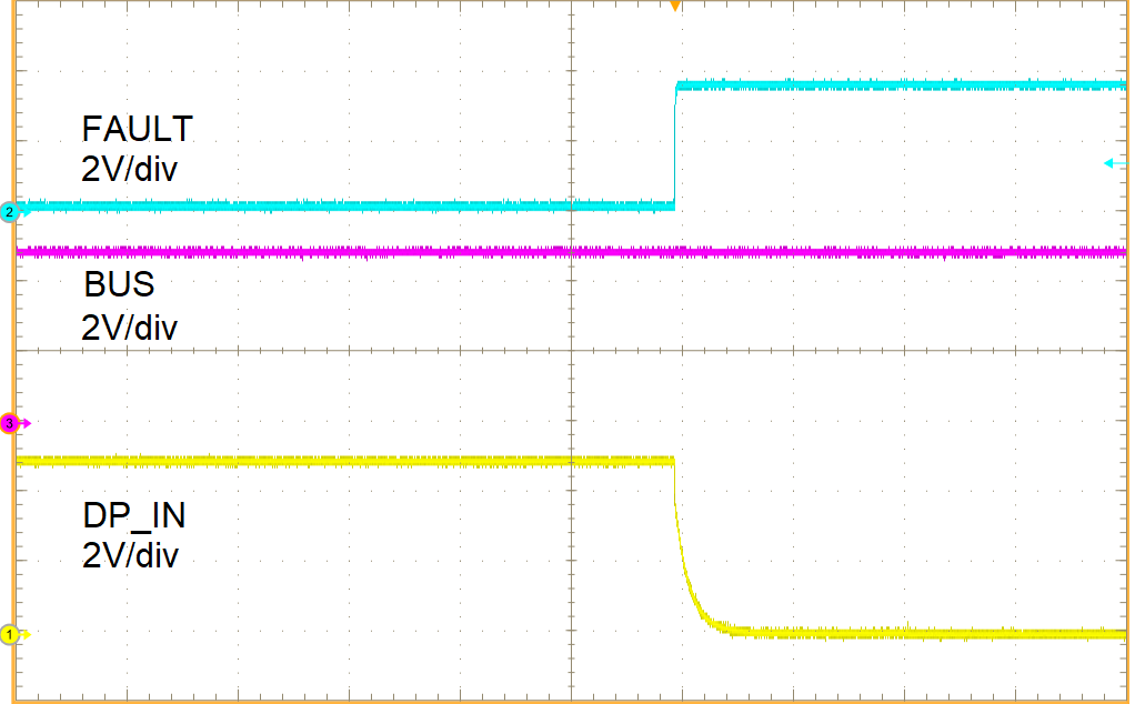
R(BIAS) = 5.1 kΩt = 20 ms/div
Figure 6-24 DP_IN Short-to-Battery Recovery
GUID-310118AC-7FE9-4713-A0C9-76BDE04D905B-low.png
R(BIAS) = 5.1 kΩt = 2 ms/div
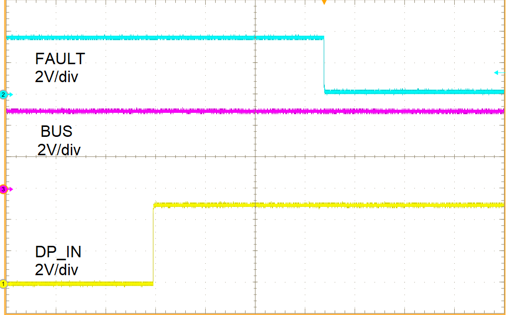
Figure 6-26 DP_IN Short-to-VBUS and Recovery
GUID-879A4DD5-692A-47F4-ACD1-E8556CB877C6-low.png
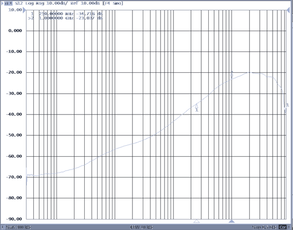
Figure 6-28 Off-State Data-Switch Isolation vs Frequency
GUID-C57A3788-A05F-45D2-B62B-40BA8467234B-low.png
Measured on EVM with 10-cm cable
Figure 6-15 Through the TPD3S713-Q1 Data Switch
GUID-414BA77B-3430-42B1-BBEC-5CCD8C2BBAB7-low.png
R(LOAD) = 68 ΩC(LOAD) = 10 µFt = 5 ms/div
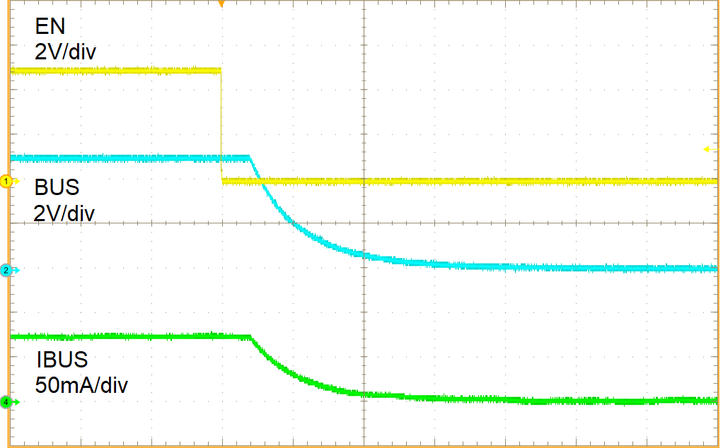
Figure 6-17 Turn-off Response
GUID-7664CD74-25C8-49A6-8177-146C9F40BDDD-low.png
R(ILIM_HI) = 80.6 kΩt = 5 ms/div
Figure 6-19 Short Circuit to No Load
GUID-9863F7F5-FD59-4338-BE96-52A6EF5EBB36-low.png
t =5 ms/div
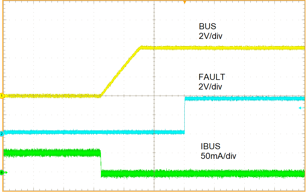
Figure 6-21 VBUS Short-to-Battery
GUID-823D8C3F-41D6-44C4-81CA-E5192DCC43C3-low.png
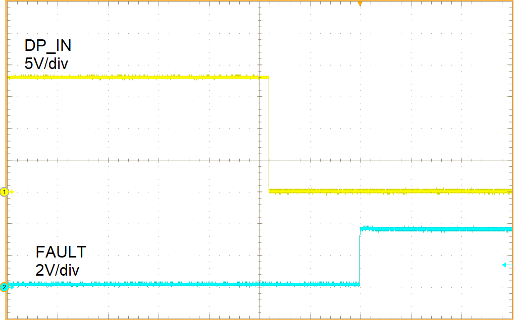
t = 5 ms/div
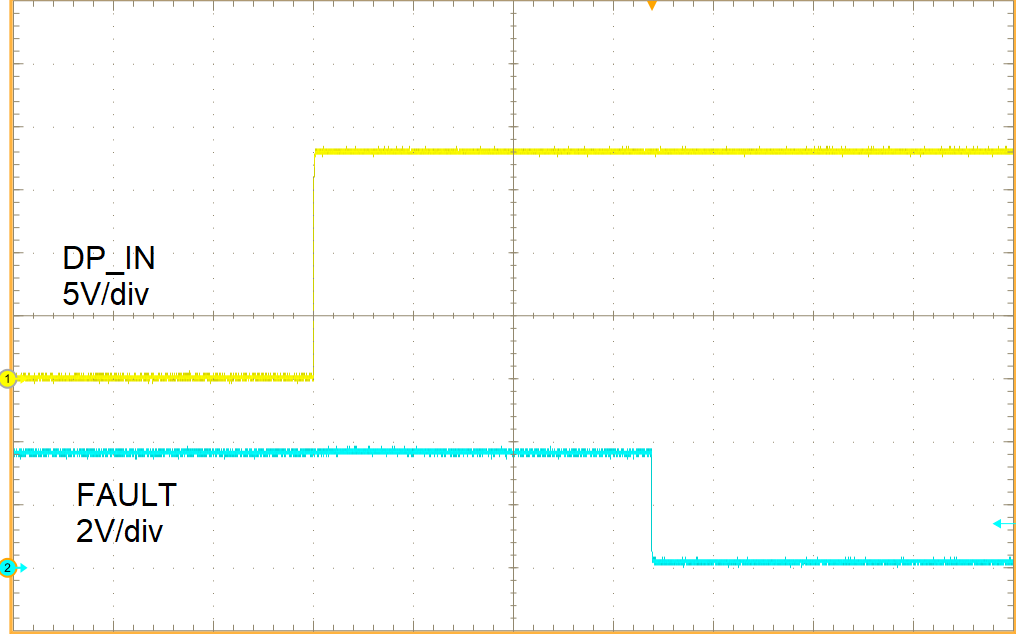
Figure 6-23 DP_IN Short-to-Battery
GUID-A863584B-5C32-4C19-BFA4-AE2F9C51A248-low.png
R(BIAS) = 5.1 kΩt = 5 ms/div
Figure 6-25 DP_IN Short-to-VBUS
GUID-5E1CEFE5-D758-4213-8052-C0D4185F3E54-low.png
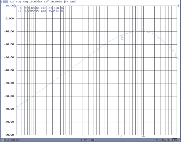
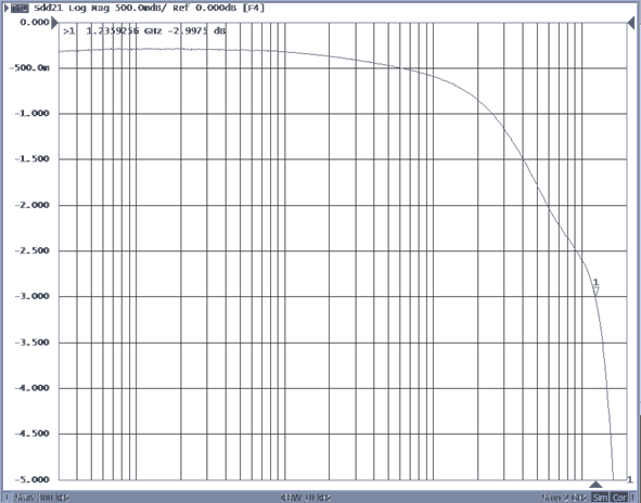
Figure 6-27 Data Transmission Characteristics vs Frequency
GUID-2B3EAD0A-CAC3-487C-A23D-26C5CCF95907-low.png
Figure 6-29 On-State Cross-Channel Isolation vs Frequency