SLVSCO7C August 2014 – September 2017 TPD1E05U06-Q1 , TPD4E05U06-Q1
PRODUCTION DATA.
- 1 Features
- 2 Applications
- 3 Description
- 4 Revision History
- 5 Pin Configuration and Functions
- 6 Specifications
- 7 Detailed Description
- 8 Application and Implementation
- 9 Layout
- 10Device and Documentation Support
- 11Mechanical, Packaging, and Orderable Information
Package Options
Mechanical Data (Package|Pins)
- DQA|10
Thermal pad, mechanical data (Package|Pins)
- DQA|10
Orderable Information
7 Detailed Description
7.1 Overview
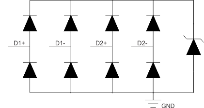
The TPDxE05U06-Q1 is a family of unidirectional TVS ESD protection diode arrays with ultra-low capacitance between 0.42 pF and 0.5 pF. They are rated to dissipate ESD strikes above the maximum level specified in the IEC 61000-4-2 level 4 international standard (12-kV contact, 15-kV air gap). The ultra-low loading capacitance makes them ideal for protecting any high-speed signal applications up to 6 Gbps.
7.2 Functional Block Diagram


7.3 Feature Description
7.3.1 AEC-Q101 Qualification
These devices are qualified to AEC-Q101 standards. They pass HBM H3B (±8 kV) and CDM C5 (±1 kV) ESD ratings and are qualified to operate from –40°C to +125°C.
7.3.2 IEC 61000-4-2 Level 4 ESD Protection
The I/O pins can withstand ESD events up to ±12-kV contact and ±15-kV air. An ESD-surge clamp diverts the current to ground.
7.3.3 IEC 61000-4-4 EFT Protection
The I/O pins can withstand an electrical fast transient burst of up to 80 A (5/50 ns waveform, 4 kV with 50-Ω impedance). An ESD-surge clamp diverts the current to ground.
7.3.4 IEC 61000-4-5 Surge Protection
The I/O pins can withstand surge events up to 2.5 A and 40 W (8/20 µs waveform). An ESD-surge clamp diverts this current to ground.
7.3.5 I/O Capacitance
The capacitance between each I/O pin to ground is 0.5 pF. These capacitances support data rates up to 5 Gbps.
7.3.6 DC Breakdown Voltage
The DC breakdown voltage of each I/O pin is a minimum of 6.4 V. This ensures that sensitive equipment is protected from surges above the reverse standoff voltage of 5 V.
7.3.7 Ultra-Low Leakage Current
The I/O pins feature an ultra-low leakage current of 10 nA (Maximum) with a bias of 2.5 V.
7.3.8 Low ESD Clamping Voltage
The I/O pins feature an ESD clamp that is capable of clamping the voltage to 10 V (IPP = 1 A).
7.3.9 Easy Flow-Through Routing
The layout of this device makes it simple and easy to add protection to an existing layout. The packages offers flow-through routing, requiring minimal modification to an existing layout.
7.4 Device Functional Modes
The TPDxE05U06-Q1 are passive integrated circuits that triggers when voltages are above VBR or below the lower diodes Vf (–0.6 V). During ESD events, voltages as high as ±15 kV (air) can be directed to ground via the internal diode network. When the voltages on the protected line fall below the trigger levels of TPDxE05U06-Q1 (usually within 10s of nano-seconds) the devices reverts to passive.