SLVSF72C December 2019 – February 2021 TPD4S311 , TPD4S311A
PRODUCTION DATA
- 1 Features
- 2 Applications
- 3 Description
- 4 Revision History
- 5 Device Comparison Table
- 6 Pin Configuration and Functions
- 7 Specifications
-
8 Detailed Description
- 8.1 Overview
- 8.2 Functional Block Diagram
- 8.3
Feature Description
- 8.3.1 4-Channels of Short-to-VBUS Overvoltage Protection (CC1, CC2, SBU1, SBU2 Pins ): 24-VDC Tolerant
- 8.3.2 4-Channels of IEC 61000-4-2 ESD Protection (CC1, CC2, SBU1, SBU2 Pins)
- 8.3.3 CC1, CC2 Overvoltage Protection FETs 400-mA or 600-mA Capable for Passing VCONN Power
- 8.3.4 CC Dead Battery Resistors Integrated for Handling the Dead Battery Use Case in Mobile Devices
- 8.3.5 1.69-mm × 1.69-mm DSBGA Package
- 8.4 Device Functional Modes
- 9 Application and Implementation
- 10Power Supply Recommendations
- 11Layout
- 12Device and Documentation Support
- 13Mechanical, Packaging, and Orderable Information
Package Options
Mechanical Data (Package|Pins)
- YBF|16
Thermal pad, mechanical data (Package|Pins)
Orderable Information
8.3.1 4-Channels of Short-to-VBUS Overvoltage Protection (CC1, CC2, SBU1, SBU2 Pins ): 24-VDC Tolerant
The TPD4S311 provides 4-channels of Short-to-VBUS Overvoltage Protection for the CC1, CC2, SBU1, and SBU2 pins of the USB Type-C connector. The TPD4S311 is able to handle 24-VDC on its C_CC1, C_CC2, C_SBU1, and C_SBU2 pins. This is necessary because according to the USB PD specification, with VBUS set for 20-V operation, the VBUS voltage is allowed to legally swing up to 21 V and 21.5 V on voltage transitions from a different USB PD VBUS voltage. The TPD4S311 builds in tolerance up to 24-VBUS to provide margin above this 21.5-V specification to be able to support USB PD adaptors that may break the USB PD specification.
When a short-to-VBUS event occurs, ringing happens due to the RLC elements in the hot-plug event. With very low resistance in this RLC circuit, ringing up to twice the settling voltage can appear on the connector. More than 2x ringing can be generated if any capacitor on the line derates in capacitance value during the short-to-VBUS event. This means that more than 44 V could be seen on a USB Type-C pin during a Short-to-VBUS event. The TPD4S311 has built in circuit protection to handle this ringing. The diode clamps used for IEC ESD protection also clamp the ringing voltage during the short-to-VBUS event to limit the peak ringing to approximately 30 V. Additionally, the overvoltage protection FETs integrated inside the TPD4S311 are 30-V tolerant, therefore being capable of supporting the high-voltage ringing waveform that is experienced during the short-to-VBUS event. The well designed combination of voltage clamps and 30-V tolerant OVP FETs insures the TPD4S311 can handle Short-to-VBUS hot-plug events with hot-plug voltages as high as 24-VDC.
The TPD4S311 has an extremely fast turnoff time of 70 ns typical. Furthermore, additional voltage clamps are placed after the OVP FET on the system side (CC1, CC2, SBU1, SBU2) pins of the TPD4S311, to further limit the voltage and current that are exposed to the USB Type-C CC/PD controller during the 70 ns interval while the OVP FET is turning off. The combination of connector side voltage clamps, OVP FETs with extremely fast turnoff time, and system side voltage clamps all work together to insure the level of stress seen on a CC1, CC2, SBU1, or SBU2 pin during a short-to-VBUS event is less than or equal to an HBM event. This is done by design, as any USB Type-C CC/PD controller will have built in HBM ESD protection.
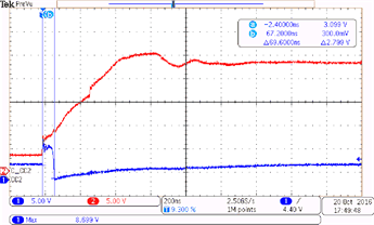
Figure 8-1 is an example of the TPD4S311 successfully protecting the TPS65982, the world's first fully integrated, full-featured USB Type-C and PD controller.
 Figure 8-1 TPD4S311 Protecting the TPS65982 During a Short-to-VBUS Event