SLIS182 November   2016 TPL0401A-10-Q1 , TPL0401B-10-Q1

PRODUCTION DATA.  

  1. Features
  2. Applications
  3. Description
  4. Revision History
  5. Device Comparison Table
  6. Pin Configuration and Functions
  7. Specifications
    1. 7.1 Absolute Maximum Ratings
    2. 7.2 ESD Ratings
    3. 7.3 Recommended Operating Conditions
    4. 7.4 Thermal Information
    5. 7.5 Electrical Characteristics
    6. 7.6 Timing Requirements
    7. 7.7 Typical Characteristics
  8. Parameter Measurement Information
  9. Detailed Description
    1. 9.1 Overview
    2. 9.2 Functional Block Diagram
    3. 9.3 Feature Description
    4. 9.4 Device Functional Modes
      1. 9.4.1 Voltage Divider Mode
    5. 9.5 Programming
      1. 9.5.1 I2C General Operation and Overview
        1. 9.5.1.1 START and STOP Conditions
        2. 9.5.1.2 Data Validity and Byte Formation
        3. 9.5.1.3 Acknowledge (ACK) and Not Acknowledge (NACK)
        4. 9.5.1.4 Repeated Start
      2. 9.5.2 Programing With I2C
        1. 9.5.2.1 Write Operation
        2. 9.5.2.2 Read Operation
    6. 9.6 Register Maps
      1. 9.6.1 Slave Address
      2. 9.6.2 Register Address
  10. 10Application and Implementation
    1. 10.1 Application Information
    2. 10.2 Typical Application
      1. 10.2.1 Design Requirements
      2. 10.2.2 Detailed Design Procedure
      3. 10.2.3 Application Curve
  11. 11Power Supply Recommendations
    1. 11.1 Power Sequence
    2. 11.2 Power-On Reset Requirements
    3. 11.3 I2C Communication After Power Up
    4. 11.4 Wiper Position While Unpowered and After Power Up
  12. 12Layout
    1. 12.1 Layout Guidelines
    2. 12.2 Layout Example
  13. 13Device and Documentation Support
    1. 13.1 Documentation Support
      1. 13.1.1 Related Documentation
    2. 13.2 Related Links
    3. 13.3 Receiving Notification of Documentation Updates
    4. 13.4 Community Resources
    5. 13.5 Trademarks
    6. 13.6 Electrostatic Discharge Caution
    7. 13.7 Glossary
  14. 14Mechanical, Packaging, and Orderable Information

Package Options

Mechanical Data (Package|Pins)
Thermal pad, mechanical data (Package|Pins)
Orderable Information

Pin Configuration and Functions

DCK Package
6-Pin SC70
Top View
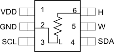
TPL0401A-10-Q1 TPL0401B-10-Q1 pos_lis144.gif

Pin Functions

PIN TYPE DESCRIPTION
NO. NAME
1 VDD Power Positive supply voltage
2 GND Ground
3 SCL I I2C Clock
4 SDA I/O I2C Data
5 W I/O Wiper terminal
6 H I/O High terminal
L I/O Low terminal (Internally connected to GND)