SLVSE19B June   2019  – November 2021 TPS1HB50-Q1

PRODUCTION DATA  

  1. Features
  2. Applications
  3. Description
  4. Revision History
  5. Device Comparison Table
  6. Pin Configuration and Functions
    1. 6.1 Recommended Connections for Unused Pins
  7. Specifications
    1. 7.1 Absolute Maximum Ratings
    2. 7.2 ESD Ratings
    3. 7.3 Recommended Operating Conditions
    4. 7.4 Thermal Information
    5. 7.5 Electrical Characteristics
    6. 7.6 SNS Timing Characteristics
    7. 7.7 Switching Characteristics
    8. 7.8 Typical Characteristics
  8. Parameter Measurement Information
  9. Detailed Description
    1. 9.1 Overview
    2. 9.2 Functional Block Diagram
    3. 9.3 Feature Description
      1. 9.3.1 Protection Mechanisms
        1. 9.3.1.1 Thermal Shutdown
        2. 9.3.1.2 Current Limit
          1. 9.3.1.2.1 Current Limit Foldback
          2. 9.3.1.2.2 Programmable Current Limit
          3. 9.3.1.2.3 Undervoltage Lockout (UVLO)
          4. 9.3.1.2.4 VBB During Short-to-Ground
        3. 9.3.1.3 Voltage Transients
          1. 9.3.1.3.1 Load Dump
          2. 9.3.1.3.2 Driving Inductive Loads
        4. 9.3.1.4 Reverse Battery
        5. 9.3.1.5 Fault Event – Timing Diagrams
      2. 9.3.2 Diagnostic Mechanisms
        1. 9.3.2.1 VOUT Short-to-Battery and Open-Load
          1. 9.3.2.1.1 Detection With Switch Enabled
          2. 9.3.2.1.2 Detection With Switch Disabled
        2. 9.3.2.2 SNS Output
          1. 9.3.2.2.1 RSNS Value
            1. 9.3.2.2.1.1 High Accuracy Load Current Sense
            2. 9.3.2.2.1.2 SNS Output Filter
        3. 9.3.2.3 Fault Indication and SNS Mux
        4. 9.3.2.4 Resistor Sharing
        5. 9.3.2.5 High-Frequency, Low Duty-Cycle Current Sensing
    4. 9.4 Device Functional Modes
      1. 9.4.1 Off
      2. 9.4.2 Standby
      3. 9.4.3 Diagnostic
      4. 9.4.4 Standby Delay
      5. 9.4.5 Active
      6. 9.4.6 Fault
  10. 10Application and Implementation
    1. 10.1 Application Information
      1. 10.1.1 Ground Protection Network
      2. 10.1.2 Interface With Microcontroller
      3. 10.1.3 I/O Protection
      4. 10.1.4 Inverse Current
      5. 10.1.5 Loss of GND
      6. 10.1.6 Automotive Standards
        1. 10.1.6.1 ISO7637-2
        2. 10.1.6.2 AEC-Q100-012 Short Circuit Reliability
      7. 10.1.7 Thermal Information
    2. 10.2 Typical Application
      1. 10.2.1 Design Requirements
      2. 10.2.2 Detailed Design Procedure
        1. 10.2.2.1 Thermal Considerations
        2. 10.2.2.2 RILIM Calculation
        3. 10.2.2.3 Diagnostics
          1. 10.2.2.3.1 Selecting the RISNS Value
  11. 11Power Supply Recommendations
  12. 12Layout
    1. 12.1 Layout Guidelines
    2. 12.2 Layout Example
  13. 13Device and Documentation Support
    1. 13.1 Documentation Support
      1. 13.1.1 Related Documentation
    2. 13.2 Receiving Notification of Documentation Updates
    3. 13.3 Support Resources
    4. 13.4 Trademarks
    5. 13.5 Electrostatic Discharge Caution
    6. 13.6 Glossary
  14. 14Mechanical, Packaging, and Orderable Information

Package Options

Mechanical Data (Package|Pins)
Thermal pad, mechanical data (Package|Pins)
Orderable Information

Typical Characteristics

GUID-184C643C-3316-42F4-BB37-6AA4699FD1AC-low.gifFigure 7-1 Transient Thermal Impedance
GUID-E44FB63D-CE15-445B-AEB4-EA16C103CBA8-low.gif
IOUT = 0 AVEN = 5 VVDIAG_EN = 5 V
RSNS = 1 kΩVSEL1 = 0 V
Figure 7-3 Quiescent Current (IQ) vs Temperature
GUID-EDF3F81A-BD2A-48F5-B342-1DD47A0FDCF0-low.gif
IOUT = 200 mAVEN = 5 VVDIAG_EN = 0 V
RSNS = 1 kΩ
Figure 7-5 On Resistance (RON) vs Temperature
GUID-2AF6B862-F87B-4360-B9AF-AE7957CF5DDD-low.gif
ROUT = 6 ΩVEN = 0 V to 5 VVDIAG_EN = 0 V
RSNS = 1 kΩVBB = 13.5 V
Figure 7-7 Turn-On Delay Time (tDR) vs Temperature
GUID-12AAFF6C-3691-4C8B-9902-814DEBE92B7C-low.gif
ROUT = 6 ΩVEN = 0 V to 5 VVDIAG_EN = 0 V
RSNS = 1 kΩVBB = 13.5 V
Figure 7-9 VOUT Slew Rate Rising (SRR) vs Temperature
GUID-8B6C57BD-D969-4FA7-8372-BB5496105126-low.gif
ROUT = 6 ΩVEN = 0 V to 5 VVDIAG_EN = 0 V
RSNS = 1 kΩVBB = 13.5 V
Figure 7-11 Turn-on Time (tON) vs Temperature
GUID-15937F6D-0817-49E1-A12A-0E477A548E14-low.gif
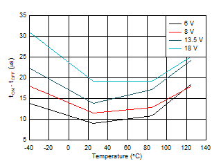
ROUT = 6 ΩVEN = 0 V to 5 V and 5 V to 0 VVDIAG_EN = 0 V
RSNS = 1 kΩVBB = 13.5 V
Figure 7-13 Turn-On and Turn-Off Matching (tON - tOFF) vs Temperature
GUID-34C08EE2-2BC3-4B2B-AF2E-979307E1C05D-low.gif
VSEL = 0 VVEN = 5 VVDIAG_EN = 5 V
RSNS = 1 kΩTA = 25°C
Figure 7-15 Current Sense Output Current (ISNSI) vs Load Current (IOUT) Across VBB
GUID-A8B8B232-E5D2-414C-B13A-7AA0962FF11C-low.gif
VSEL = 0 VVEN = 0 VVDIAG_EN = 5 V
RSNS = 1 kΩVOUT Floating
Figure 7-17 Fault High Output Current (ISNSFH) vs Temperature
GUID-02A11E5E-3FCC-436F-87C3-E72109C728D6-low.gif
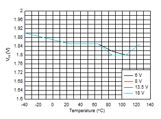
VEN = 0 V to 3.3 VVOUT = 13.5 VVDIAG_EN = 0 V
ROUT = 1 kΩVBB = 13.5 V
Figure 7-19 VIH vs Temperature
GUID-392E6822-D3B1-455C-8BCA-0EC99BF57788-low.gif
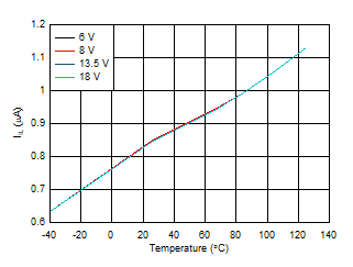
VEN = 0.8 VVOUT = 0 VVDIAG_EN = 0 V
ROUT = 1 kΩVBB = 13.5 V
Figure 7-21 IIL vs Temperature
GUID-EBE27517-A7B3-4941-9C95-64CD16F0F1AB-low.png
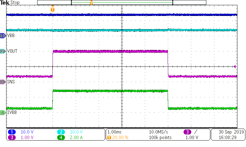
ROUT = 6 ΩRSNS = 1 kΩVDIA_EN = 5 V
VSEL = 0 V
Figure 7-23 Turn-On Time (tON)
GUID-57406745-0790-4C81-8D56-CFF736FE317C-low.png
ROUT =13 Ω to 6 ΩRSNS = 1 kΩVSEL = 0 V
IOUT = 1 A to 3 AVBB = 13.5 V
Figure 7-25 ISNS Settling Time (tSNSION1) on Load Step
GUID-F6A042C9-27D2-48F3-846A-D61A2C713E46-low.png
LOUT = 5 µH to GNDRLIM = 5 kΩVSEL = 0 V
VEN = 0 V to 5 VVDIAG_EN = 5 VTA = 25°C
Figure 7-27 Device Version A Short Circuit Event
GUID-2F0ADE72-2EB9-4313-A3DB-CDF28ED361E8-low.png
VBB = 13.5 V TA = 25°C LOUT = 5 mH
Figure 7-29 5-mH Inductive Load Demagnetization
GUID-B0C1826D-7982-4651-BC5F-73B2D773381A-low.gif
VOUT = 0 VVEN = 0 VVDIAG_EN = 0 V
Figure 7-2 Standby Current (ISB) vs Temperature
GUID-23BDD3E1-CD6E-44E3-975C-4C363CA111F9-low.gif
IOUT = 0 AVEN = 0 VVDIAG_EN = 5 V
RSNS = 1 kΩVSEL1 = 0 V
Figure 7-4 Diag Enable Current (IDIA) vs Temperature
GUID-6EA55135-A788-4958-8B29-BF2FDA48ED89-low.gif
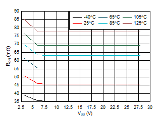
IOUT = 200 mAVEN = 5 VVDIAG_EN = 0 V
RSNS = 1 kΩ
Figure 7-6 On Resistance (RON) vs VBB
GUID-F790F486-26D4-4C75-AACB-98703F4441FA-low.gif
ROUT = 6 ΩVEN = 5 V to 0 VVDIAG_EN = 0 V
RSNS = 1 kΩVBB = 13.5 V
Figure 7-8 Turn-Off Delay Time (tDF) vs Temperature
GUID-8FE5750B-2F4C-432D-914E-1C43A6386002-low.gif
ROUT = 6 ΩVEN = 5 V to 0 VVDIAG_EN = 0 V
RSNS = 1 kΩVBB = 13.5 V
Figure 7-10 VOUT Slew Rate Falling (SRF) vs Temperature
GUID-1960038B-21D7-4662-8920-D55AD4D47A04-low.gif
ROUT = 6 ΩVEN = 5 V to 0 VVDIAG_EN = 0 V
RSNS = 1 kΩVBB = 13.5 V
Figure 7-12 Turn-Off Time (tOFF) vs Temperature
GUID-7E8B78C0-4A9F-4D19-98D0-28E7A41163BC-low.gif
VSEL = 0 VVEN = 5 VVDIAG_EN = 5 V
RSNS = 1 kΩVBB = 13.5 V
Figure 7-14 Current Sense Output Current (ISNSI ) vs Load Current (IOUT) Across Temperature
GUID-71148A25-FBAB-46C8-A93E-7E9AB408B2CE-low.gif
VSEL = 5 VVEN = 0 VVDIAG_EN = 5 V
RSNS = 1 kΩ
Figure 7-16 Temperature Sense Output Current (ISNST) vs Temperature
GUID-B3A911AC-3A30-4CF9-9C29-2209CCB50F51-low.gif
VEN = 3.3 V to 0 VVOUT = 0 VVDIAG_EN = 0 V
ROUT = 1 kΩVBB = 13.5 V
Figure 7-18 VIL vs Temperature
GUID-8B608D00-02AD-4C5C-9118-17DF36F099B2-low.gif
VEN = 0 V to 3.3 V and 3.3 V to 0 VVOUT = 0 VVDIAG_EN = 0 V
ROUT = 1 kΩVBB = 13.5 V
Figure 7-20 VHYST vs Temperature
GUID-B2D80788-D1AB-49A4-BD7F-47B372127223-low.gif
VEN = 5 VVOUT = 13.5V VVDIAG_EN = 0 V
ROUT = 1 kΩVBB = 13.5 V
Figure 7-22 IIH vs Temperature
GUID-7B6CE288-DAEE-49A0-BBF8-E6FC029C2D99-low.png
ROUT = 6 ΩRSNS = 1 kΩVDIA_EN = 5 V
VSEL = 0 V
Figure 7-24 Turn-Off Time (tOFF)
GUID-4FB5D732-0CF1-4F1D-A06D-89FD8CD6BE67-low.png
VBB = 13.5 VTA = 25°CIOUT = 3 A
VEN = 0 V to 5 V
Figure 7-26 SNS Output Current Measurement Enable on DIAG_EN PWM
GUID-5C9595FA-6D48-4622-8F61-1C5D0B965183-low.png
LOUT = 5 µH to GNDRLIM = 5 kΩVSEL = 0 V
VEN = 0 V to 5 VVDIAG_EN = 5 VTA = 25°C
Figure 7-28 Device Version B Short Circuit Event