SLVSHZ1 June 2024 TPS1HTC100-Q1
PRODUCTION DATA
- 1
- 1 Features
- 2 Applications
- 3 Description
- 4 Pin Configuration and Functions
- 5 Specifications
- 6 Parameter Measurement Information
- 7 Detailed Description
- 8 Application and Implementation
- 9 Device and Documentation Support
- 10Revision History
- 11Mechanical, Packaging, and Orderable Information
Package Options
Mechanical Data (Package|Pins)
- PWP|14
Thermal pad, mechanical data (Package|Pins)
- PWP|14
Orderable Information
7.3.3 Inductive-Load Switching-Off Clamp
When an inductive load is switching off, the output voltage is pulled down to negative, due to the inductance characteristics. The power FET can break down if the voltage is not clamped during the current decay period. To protect the power FET in this situation, an internal drain to gate clamp, namely the VDS,clamp is used to clamp the voltage between the drain and source of the device.

During the current-decay period (TDECAY), the power FET is turned on for inductive energy dissipation. Both the energy of the power supply (EBAT) and the load (ELOAD) are dissipated on the high-side power switch itself, which is called EHSD. If resistance is in series with inductance, some of the load energy is dissipated in the resistance.

From the high-side power switch view, EHSD equals the integration value during the current decay period.
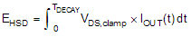
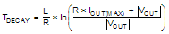
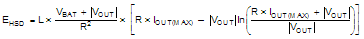
When R approximately equals 0, EHSD can be given simply as:
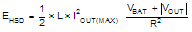
 Figure 7-4 Driving
Inductive Load
Figure 7-4 Driving
Inductive Load Figure 7-5 Inductive-Load Switching-Off Diagram
As discussed previously, when switching off, battery energy and load energy are dissipated on the high-side power switch, which leads to the large thermal variation. For each high-side power switch, the upper limit of the maximum safe power dissipation depends on the device intrinsic capacity, ambient temperature, and board dissipation condition.