SLVS514P April   2004  – August 2024 TPS2041B , TPS2042B , TPS2043B , TPS2044B , TPS2051B , TPS2052B , TPS2053B , TPS2054B

PRODUCTION DATA  

  1.   1
  2. Features
  3. Applications
  4. Description
  5. General Switch Catalog
  6. Pin Configuration and Functions
  7. Specifications
    1. 6.1 Absolute Maximum Ratings
    2. 6.2 ESD Ratings
    3. 6.3 Recommended Operating Conditions
    4. 6.4 Thermal Information
    5. 6.5 Electrical Characteristics
    6. 6.6 Typical Characteristics (All Devices Excluding TPS2051BDBV and TPS2052BD)
    7. 6.7 Typical Characteristics (TPS2051BDBV and TPS2052BD)
  8. Parameter Measurement Information
  9. Detailed Description
    1. 8.1 Overview
    2. 8.2 Functional Block Diagrams
    3. 8.3 Feature Description
      1. 8.3.1  Power Switch
      2. 8.3.2  Charge Pump
      3. 8.3.3  Driver
      4. 8.3.4  Enable ( ENx)
      5. 8.3.5  Enable (ENx)
      6. 8.3.6  Current Sense
      7. 8.3.7  Overcurrent
        1. 8.3.7.1 Overcurrent Conditions (TPS20x3BD, TPS20x4BD, and TPS20x2BDRB)
        2. 8.3.7.2 Overcurrent Conditions (TPS20x1B & TPS20x2B in D, DGN, and DBV packages)
      8. 8.3.8  Overcurrent ( OCx)
      9. 8.3.9  Thermal Sense
      10. 8.3.10 Undervoltage Lockout
    4. 8.4 Device Functional Modes
  10. Application and Implementation
    1. 9.1 Application Information
      1. 9.1.1 Universal Serial Bus (USB) Applications
    2. 9.2 Typical Application
      1. 9.2.1 Typical Application (TPS2042B)
        1. 9.2.1.1 Design Requirements
        2. 9.2.1.2 Detailed Design Procedure
          1. 9.2.1.2.1 Power-Supply Considerations
          2. 9.2.1.2.2 OC Response
        3. 9.2.1.3 Application Curves
      2. 9.2.2 Host and Self-Powered and Bus-Powered Hubs
        1. 9.2.2.1 Design Requirements
          1. 9.2.2.1.1 USB Power-Distribution Requirements
        2. 9.2.2.2 Detailed Design Procedure
          1. 9.2.2.2.1 Low-Power Bus-Powered and High-Power Bus-Powered Functions
        3. 9.2.2.3 Application Curves
      3. 9.2.3 Generic Hot-Plug Applications
        1. 9.2.3.1 Design Requirements
        2. 9.2.3.2 Detailed Design Procedure
        3. 9.2.3.3 Application Curves
  11. 10Power Supply Recommendations
    1. 10.1 Undervoltage Lockout (UVLO)
  12. 11Layout
    1. 11.1 Layout Guidelines
    2. 11.2 Layout Example
    3. 11.3 Power Dissipation
    4. 11.4 Thermal Protection
  13. 12Device and Documentation Support
    1. 12.1 Receiving Notification of Documentation Updates
    2. 12.2 Support Resources
    3. 12.3 Trademarks
    4. 12.4 Electrostatic Discharge Caution
    5. 12.5 Glossary
  14. 13Revision History
  15. 14Mechanical, Packaging, and Orderable Information

Package Options

Mechanical Data (Package|Pins)
Thermal pad, mechanical data (Package|Pins)
Orderable Information

Typical Characteristics (All Devices Excluding TPS2051BDBV and TPS2052BD)

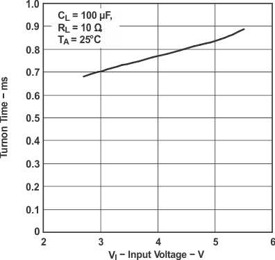
TPS2041B TPS2042B TPS2043B TPS2044B  TPS2051B TPS2052B TPS2053B TPS2054B Turnon Time vs Input Voltage
Figure 6-1 Turnon Time vs Input Voltage
TPS2041B TPS2042B TPS2043B TPS2044B  TPS2051B TPS2052B TPS2053B TPS2054B Rise Time vs Input Voltage
Figure 6-3 Rise Time vs Input Voltage
TPS2041B TPS2042B TPS2043B TPS2044B  TPS2051B TPS2052B TPS2053B TPS2054B TPS20x2BDRB Supply
                                                  Current, Output Enabled vs Junction
                                                  Temperature
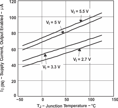
\
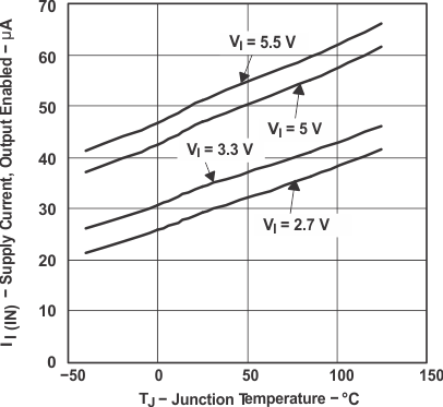
Figure 6-5 TPS20x2BDRB Supply Current, Output Enabled vs Junction Temperature
TPS2041B TPS2042B TPS2043B TPS2044B  TPS2051B TPS2052B TPS2053B TPS2054B TPS2044B TPS2054B Supply Current, Output Enabled vs Junction Temperature
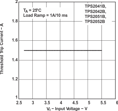
Figure 6-7 TPS2044B TPS2054B Supply Current, Output Enabled vs Junction Temperature
TPS2041B TPS2042B TPS2043B TPS2044B  TPS2051B TPS2052B TPS2053B TPS2054B TPS2043B and TPS2053B Supply Current, Output Disabled vs Junction Temperature
Figure 6-9 TPS2043B and TPS2053B Supply Current, Output Disabled vs Junction Temperature
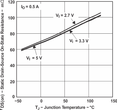
TPS2041B TPS2042B TPS2043B TPS2044B  TPS2051B TPS2052B TPS2053B TPS2054B Static Drain-Source on-State Resistance vs Junction Temperature
Figure 6-11 Static Drain-Source on-State Resistance vs Junction Temperature
TPS2041B TPS2042B TPS2043B TPS2044B  TPS2051B TPS2052B TPS2053B TPS2054B Threshold Trip Current
                                                  vs Input Voltage
Figure 6-13 Threshold Trip Current vs Input Voltage
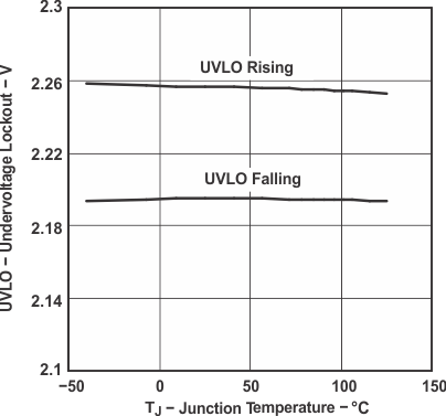
TPS2041B TPS2042B TPS2043B TPS2044B  TPS2051B TPS2052B TPS2053B TPS2054B Undervoltage Lockout vs Junction Temperature
Figure 6-15 Undervoltage Lockout vs Junction Temperature
TPS2041B TPS2042B TPS2043B TPS2044B  TPS2051B TPS2052B TPS2053B TPS2054B Turnon Delay and Rise Time With 1-µF Load
Figure 6-17 Turnon Delay and Rise Time With 1-µF Load
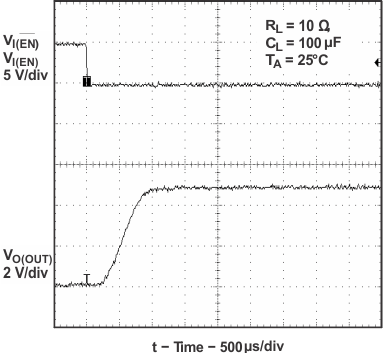
TPS2041B TPS2042B TPS2043B TPS2044B  TPS2051B TPS2052B TPS2053B TPS2054B Turnon Delay and Rise Time With 100-µF Load
Figure 6-19 Turnon Delay and Rise Time With 100-µF Load
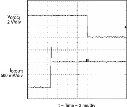
TPS2041B TPS2042B TPS2043B TPS2044B  TPS2051B TPS2052B TPS2053B TPS2054B Short-Circuit Current,  Device Enabled Into Short
Figure 6-21 Short-Circuit Current, Device Enabled Into Short
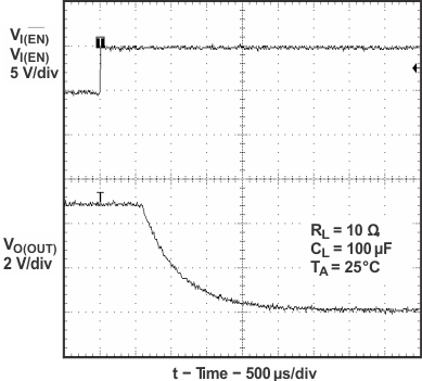
TPS2041B TPS2042B TPS2043B TPS2044B  TPS2051B TPS2052B TPS2053B TPS2054B 3-Ω Load Connected to Enabled Device
Figure 6-23 3-Ω Load Connected to Enabled Device
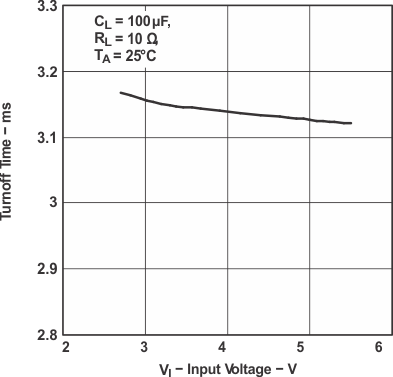
TPS2041B TPS2042B TPS2043B TPS2044B  TPS2051B TPS2052B TPS2053B TPS2054B Turnoff Time vs Input Voltage
Figure 6-2 Turnoff Time vs Input Voltage
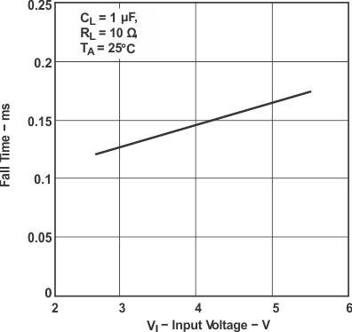
TPS2041B TPS2042B TPS2043B TPS2044B  TPS2051B TPS2052B TPS2053B TPS2054B Fall Time vs Input Voltage
\
Figure 6-4 Fall Time vs Input Voltage
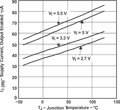
TPS2041B TPS2042B TPS2043B TPS2044B  TPS2051B TPS2052B TPS2053B TPS2054B TPS2043B and TPS2053B Supply Current, Output Enabled vs Junction Temperature
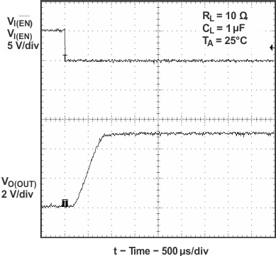
Figure 6-6 TPS2043B and TPS2053B Supply Current, Output Enabled vs Junction Temperature
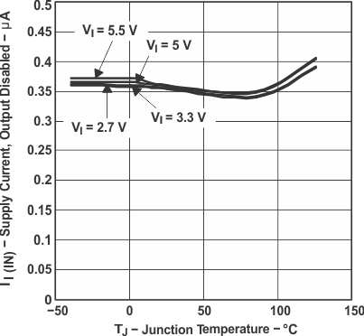
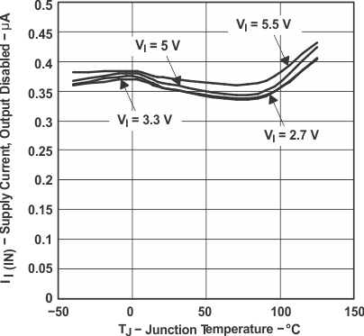
TPS2041B TPS2042B TPS2043B TPS2044B  TPS2051B TPS2052B TPS2053B TPS2054B TPS20x2BDRB Supply
                                                  Current, Output Disabled vs Junction
                                                  Temperature
Figure 6-8 TPS20x2BDRB Supply Current, Output Disabled vs Junction Temperature
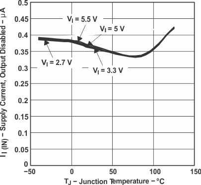
TPS2041B TPS2042B TPS2043B TPS2044B  TPS2051B TPS2052B TPS2053B TPS2054B TPS2044B and TPS2054B Supply Current, Output Disabled vs Junction Temperature
Figure 6-10 TPS2044B and TPS2054B Supply Current, Output Disabled vs Junction Temperature
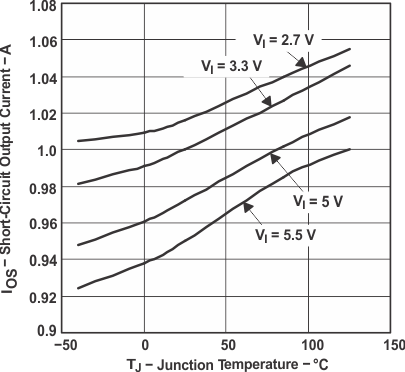
TPS2041B TPS2042B TPS2043B TPS2044B  TPS2051B TPS2052B TPS2053B TPS2054B Short-Circuit Output Current vs Junction Temperature
Figure 6-12 Short-Circuit Output Current vs Junction Temperature
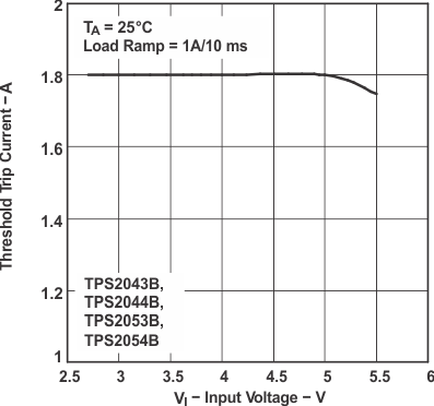
TPS2041B TPS2042B TPS2043B TPS2044B  TPS2051B TPS2052B TPS2053B TPS2054B Threshold Trip Current vs Input Voltage
Figure 6-14 Threshold Trip Current vs Input Voltage
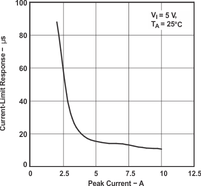
TPS2041B TPS2042B TPS2043B TPS2044B  TPS2051B TPS2052B TPS2053B TPS2054B Current-Limit Response vs Peak Current
Figure 6-16 Current-Limit Response vs Peak Current
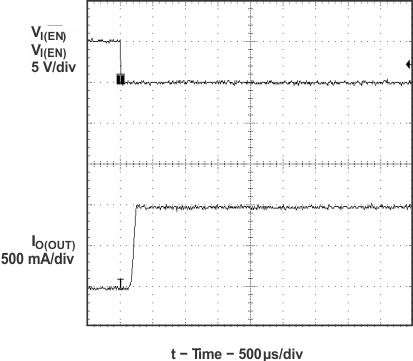
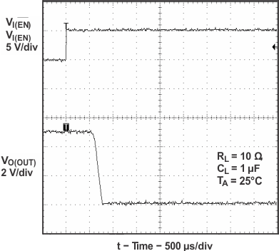
TPS2041B TPS2042B TPS2043B TPS2044B  TPS2051B TPS2052B TPS2053B TPS2054B Turnoff Delay and Fall Time With 1-µF Load
Figure 6-18 Turnoff Delay and Fall Time With 1-µF Load
TPS2041B TPS2042B TPS2043B TPS2044B  TPS2051B TPS2052B TPS2053B TPS2054B Turnoff Delay and Fall Time With 100-µF Load
Figure 6-20 Turnoff Delay and Fall Time With 100-µF Load
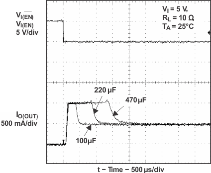
TPS2041B TPS2042B TPS2043B TPS2044B  TPS2051B TPS2052B TPS2053B TPS2054B Inrush Current With Different  Load Capacitance
Figure 6-22 Inrush Current With Different Load Capacitance
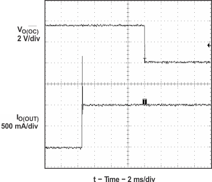
TPS2041B TPS2042B TPS2043B TPS2044B  TPS2051B TPS2052B TPS2053B TPS2054B 2-Ω Load Connected to Enabled Device
Figure 6-24 2-Ω Load Connected to Enabled Device