SLVS490K December 2003 – June 2024 TPS2061 , TPS2062 , TPS2063 , TPS2065 , TPS2066 , TPS2067
PRODUCTION DATA
- 1
- 1 Features
- 2 Applications
- 3 Description
- 4 Description (continued)
- 5 Pin Configuration and Functions
- 6 Specifications
- 7 Parameter Measurement Information
- 8 Detailed Description
-
9 Application and Implementation
- 9.1
Application Information
- 9.1.1 Power-supply Considerations
- 9.1.2 OC Response
- 9.1.3 Power Dissipation and Junction Temperature
- 9.1.4 Thermal Protection
- 9.1.5 Undervoltage Lockout (UVLO)
- 9.1.6 Universal Serial Bus (USB) Applications
- 9.1.7 Host/Self-Powered and Bus-powered Hubs
- 9.1.8 Low-power Bus-powered and High-Power Bus-Powered Functions
- 9.1.9 USB Power-distribution Requirements
- 9.1.10 Generic Hot-Plug Applications
- 9.1
Application Information
- 10Device and Documentation Support
- 11Revision History
- 12Mechanical, Packaging, and Orderable Information
Package Options
Refer to the PDF data sheet for device specific package drawings
Mechanical Data (Package|Pins)
- D|8
- DGN|8
Thermal pad, mechanical data (Package|Pins)
- DGN|8
Orderable Information
6.6 Typical Characteristics (TPS2063 & TPS2067)
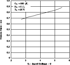 Figure 6-19 TURNON TIME vs INPUT
VOLTAGE
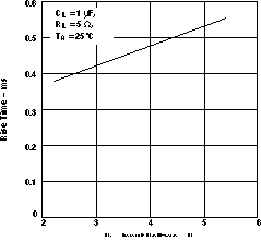 Figure 6-21 RISE TIME vs INPUT
VOLTAGE
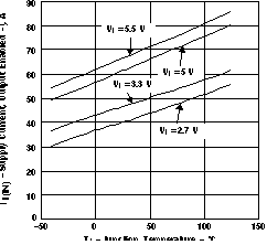 Figure 6-23 TPS2063, TPS2067 SUPPLY
CURRENT, OUTPUT ENABLED vs JUNCTION TEMPERATURE
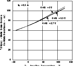 Figure 6-25 STATIC DRAIN-SOURCE
ON-STATE RESISTANCE vs JUNCTION TEMPERATURE
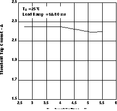 Figure 6-27 THRESHOLD TRIP CURRENT vs
INPUT VOLTAGE
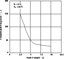 Figure 6-29 CURRENT-LIMIT RESPONSE vs
PEAK CURRENT
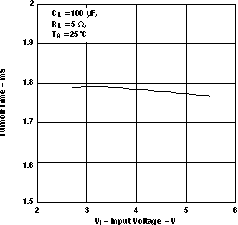 Figure 6-20 TURNOFF TIME vs INPUT
VOLTAGE
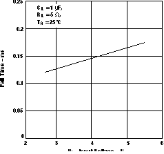 Figure 6-22 FALL TIME vs INPUT
VOLTAGE
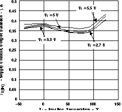 Figure 6-24 TPS2063, TPS2067 SUPPLY
CURRENT, OUTPUT DISABLED vs JUNCTION TEMPERATURE
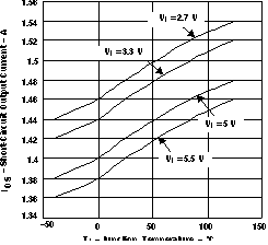 Figure 6-26 SHORT-CIRCUIT OUTPUT
CURRENT vsJUNCTION TEMPERATURE
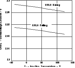 Figure 6-28 UNDERVOLTAGE LOCKOUT vs
JUNCTION TEMPERATURE
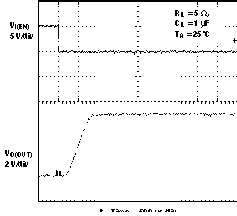 Figure 6-30 Turnon Delay and Rise Time With 1-μF Load
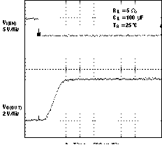 Figure 6-32 Turnon Delay and Rise Time With 100-μF Load
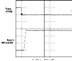 Figure 6-34 Short-Circuit Current, Device Enabled Into Short
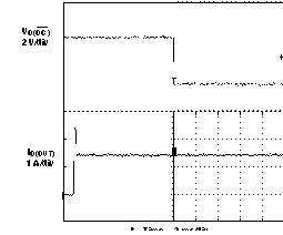 Figure 6-36 2-Ω
Load Connected to Enabled Device
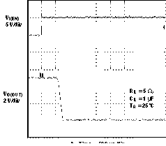 Figure 6-31 Turnoff Delay and Fall Time With 1-μF Load
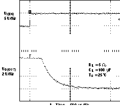 Figure 6-33 Turnoff Delay and Fall Time With 100-μF Load
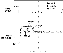 Figure 6-35 Inrush Current With Different Load Capacitance
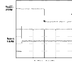 Figure 6-37 1-Ω
Load Connected to Enabled Device