SLVS798G January 2008 – June 2024 TPS2062A , TPS2066A
PRODUCTION DATA
- 1
- 1 Features
- 2 Applications
- 3 Description
- 4 Pin Configuration and Functions
- 5 Specifications
- 6 Parameter Measurement Information
- 7 Detailed Description
- 8 Application Information
- 9 Device and Documentation Support
- 10Revision History
- 11Mechanical, Packaging, and Orderable Information
Package Options
Mechanical Data (Package|Pins)
Thermal pad, mechanical data (Package|Pins)
- DRB|8
Orderable Information
4 Pin Configuration and Functions
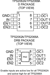
Table 4-1 Terminal Functions
| TERMINAL | I/O | DESCRIPTION | ||
|---|---|---|---|---|
| NAME | TPS2062A | TPS2066A | ||
| EN1 | 3 | — | I | Enable input, logic low turns on power switch IN-OUT1 |
| EN2 | 4 | — | I | Enable input, logic low turns on power switch IN-OUT2 |
| EN1 | — | 3 | I | Enable input, logic high turns on power switch IN-OUT1 |
| EN2 | — | 4 | I | Enable input, logic high turns on power switch IN-OUT2 |
| GND | 1 | 1 | Ground | |
| IN | 2 | 2 | I | Input voltage |
| OC1 | 8 | 8 | O | Channel 1 over-current indicator; the output is open-drain, active low type |
| OC2 | 5 | 5 | O | Channel 2 over-current indicator; the output is open-drain, active low type |
| OUT1 | 7 | 7 | O | Power-switch output, IN-OUT1 |
| OUT2 | 6 | 6 | O | Power-switch output, IN-OUT2 |
| PowerPAD™(1) | PAD | PAD | Connect PowerPAD to GND for proper operation (DRB package only) | |
(1) The PowePad must be connected externally to GND pin to meet qualifying
conditions for CB Certificate (DRB package only)