SBVS124A November 2008 – May 2016 TPS2115A-Q1
PRODUCTION DATA.
- 1 Features
- 2 Applications
- 3 Description
- 4 Revision History
- 5 Pin Configuration and Functions
- 6 Specifications
- 7 Parameter Measurement Information
- 8 Detailed Description
- 9 Application and Information
- 10Power Supply Recommendations
- 11Layout
- 12Device and Documentation Support
- 13Mechanical, Packaging, and Orderable Information
Package Options
Mechanical Data (Package|Pins)
- PW|8
Thermal pad, mechanical data (Package|Pins)
Orderable Information
9 Application and Information
NOTE
Information in the following applications sections is not part of the TI component specification, and TI does not warrant its accuracy or completeness. TI’s customers are responsible for determining suitability of components for their purposes. Customers should validate and test their design implementation to confirm system functionality.
9.1 Application Information
Some applications have two energy sources, one of which should be used in preference to another. The TPS2115A-Q1 allows either manual or automatic selection of the input supply depending on the device configuration and use in the specific application.
Figure 20 shows a circuit that connects IN1 to OUT until IN1 falls below a user-specified value. Once the voltage on IN1 falls below this value, the TPS2115A-Q1 device selects the higher of the two supplies. This usually means the TPS2115A-Q1 device swaps to the IN2 supply.
 Figure 20. Auto-Selecting for a Dual Power Supply Application
In Figure 21, the multiplexer selects between two power supplies based upon the D1 logic signal. OUT connects to IN1 if D1 is logic 1; otherwise, OUT connects to IN2. The logic thresholds for the D1 terminal are compatible with both TTL and CMOS logic.
 Figure 21. Manually Switching Power Sources
9.2 Typical Application
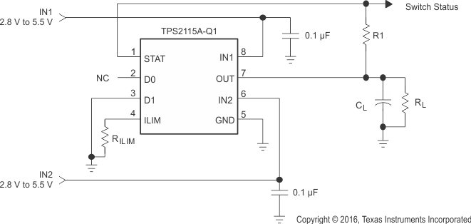
Figure 22 shows a circuit that connects IN1 to OUT until the voltage at IN1 falls below the voltage at IN2. Once the voltage on IN1 falls below the voltage on IN2, the TPS2115A-Q1 device selects IN2 since it is the higher of the two supplies.
 Figure 22. Auto-Selecting for a Dual Power Supply Application with 5 V for Normal Operation and 3.3 V Low Power Mode
9.2.1 Design Requirements
The application has two supply rails, the main supply is for normal operation with higher system current, bias current, and operation at 5 V. In this system, the second supply is needed for lower voltage, 3.3 V, with lower bias current during low-power mode. In addition, when the system enters low power mode, the other loads on the main supply need to be off. A power multiplexer is needed to connect the load automatically to the second supply when the system enters low-power mode keeping the load powered in low-power mode with minimal bias current. The load is equivalent to 50 Ω and the current limit should be set no higher than 1 A.
9.2.2 Detailed Design Procedure
The following steps are the detailed design procedure.
- Connect the main power supply, 5 V, to IN1.
- Connect the second 3.3-V supply to IN2 for the low-power mode.
- Place local bypass capacitors of 0.1 μA on IN1 and IN2 to GND to minimize ripple during transition between the power supply inputs.
- Leave D0 floating (unconnected). The internal pullup current source to Internal VDD puts a logic high on the D0 pin.
- Connect D1 to GND, logic low. The logic combination on D0 and D1 puts the device into Auto-Switching Mode.
- The application load, RL, is 50 Ω as given in the design requirements. Use a bulk capacitance, CL, of 1 μF to buffer the output voltage from dropping on OUT during the transition between IN1 and IN2.
During normal operation of the system, the main power supply connected to IN1 is on and supplies 5 V. The voltage on IN1 is higher than IN2, so the path automatically selects IN1 to OUT and the device supplies the load, RL (50 Ω), from IN1.
For low-power mode, the system turns off the main supply. The device automatically switches to the path of IN2 to OUT and the device supplies the load, RL (50 Ω), from IN2 as soon as the voltage on IN1 is lower than the voltage on IN2.
To return to normal operation, the system turns on the main supply and when the voltage on IN1 is higher than the voltage on IN2, the path automatically selects IN1 to OUT and the device supplies the load, RL (50 Ω), from IN1.
- To set the current limit below 1 A, use an RILIM of 700 Ω according to Equation 1.
- Using the current limit accuracy in the electrical characteristics section, using RILIM of 700 Ω has a maximum current limit of 0.99 A, which is below the design requirement of 1 A.

Connect a pullup resistor, R1, of 10 kΩ, to the host processor to monitor which input supply is selected.
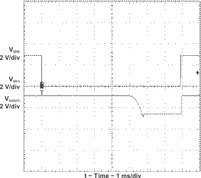
9.2.3 Application Curve
