SLVSGU5A April 2022 – July 2022 TPS22811
PRODUCTION DATA
- 1 Features
- 2 Applications
- 3 Description
- 4 Revision History
- 5 Pin Configuration and Functions
- 6 Specifications
-
7 Detailed Description
- 7.1 Overview
- 7.2 Functional Block Diagram
- 7.3
Feature Description
- 7.3.1 Undervoltage Lockout (UVLO and UVP)
- 7.3.2 Overvoltage Lockout (OVLO)
- 7.3.3 Inrush Current, Overcurrent, and Short-Circuit Protection
- 7.3.4 Analog Load Current Monitor
- 7.3.5 Overtemperature Protection (OTP)
- 7.3.6 Fault Response
- 7.3.7 Power-Good Indication (PG)
- 7.3.8 Quick Output Discharge (QOD)
- 7.4 Device Functional Modes
- 8 Application and Implementation
- 9 Power Supply Recommendations
- 10Layout
- 11Device and Documentation Support
- 12Mechanical, Packaging, and Orderable Information
Package Options
Mechanical Data (Package|Pins)
- RPW|10
Thermal pad, mechanical data (Package|Pins)
Orderable Information
3 Description
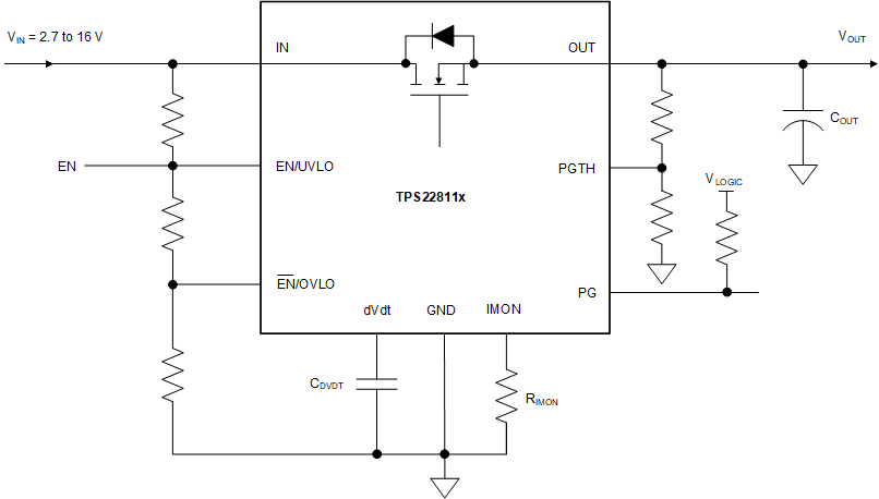
The TPS22811x is a highly-integrated, power-distribution solution in a small package. The device allows control and monitoring of power supply rails using minimum number of external components.
Output slew rate and inrush current can be adjusted using one external capacitor. Loads are protected from input overvoltage conditions by cutting off the output if input exceeds an adjustable overvoltage threshold. The device integrates a fast-trip response to provide protection against severe faults at the output during steady-state.
The devices provide an accurate analog sense of the output load current as well as a digital power-good indication to help with system monitoring and diagnostics.
The devices are available in a 2-mm × 2-mm, 10-pin HotRod™ QFN package for improved thermal performance and reduced system footprint.
The devices are characterized for operation over a junction temperature range of –40°C to +125°C.
| PART NUMBER | PACKAGE(1) | BODY SIZE (NOM) |
|---|---|---|
| TPS22811 | RPW (VQFN-HR, 10) | 2.00 mm × 2.00 mm |
 Simplified Schematic