SLVSBT4A May 2013 – August 2015 TPS22924D
PRODUCTION DATA.
- 1 Features
- 2 Applications
- 3 Description
- 4 Revision History
- 5 Pin Configuration and Functions
- 6 Specifications
- 7 Parametric Measurement Information
- 8 Detailed Description
- 9 Application and Implementation
- 10Power Supply Recommendations
- 11Layout
- 12Device and Documentation Support
- 13Mechanical, Packaging, and Orderable Information
Package Options
Mechanical Data (Package|Pins)
- YZP|6
Thermal pad, mechanical data (Package|Pins)
Orderable Information
6 Specifications
6.1 Absolute Maximum Ratings (1)
| MIN | MAX | UNIT | ||||
|---|---|---|---|---|---|---|
| VIN | Input voltage | –0.3 | 4 | V | ||
| VOUT | Output voltage | VIN + 0.3 | V | |||
| VON | ON pin voltage | –0.3 | 4 | V | ||
| IMAX | Maximum continuous switch current, TA = -40°C to 85°C | 2 | A | |||
| IPLS | Maximum pulsed switch current, 100-µs pulse, 2% duty cycle, TA = -40°C to 85°C | 4 | A | |||
| TA | Operating free-air temperature | –40 | 85 | °C | ||
| Tstg | Storage temperature | –65 | 150 | °C | ||
(1) Stresses beyond those listed under Absolute Maximum Ratings may cause permanent damage to the device. These are stress ratings only, which do not imply functional operation of the device at these or any other conditions beyond those indicated under Recommended Operating Conditions. Exposure to absolute-maximum-rated conditions for extended periods may affect device reliability.
6.2 ESD Ratings
| VALUE | UNIT | |||
|---|---|---|---|---|
| V(ESD) | Electrostatic discharge | Human body model (HBM), per ANSI/ESDA/JEDEC JS-001 (1) | ±5000 | V |
| Charged-device model (CDM), per JEDEC specification JESD22-C101 (2) | ±1000 | |||
(1) JEDEC document JEP155 states that 500-V HBM allows safe manufacturing with a standard ESD control process.
(2) JEDEC document JEP157 states that 250-V CDM allows safe manufacturing with a standard ESD control process.
6.3 Recommended Operating Conditions
| MIN | MAX | UNIT | |||
|---|---|---|---|---|---|
| VIN | Input voltage | 0.75 | 3.6 | V | |
| VOUT | Output voltage | VIN | V | ||
| VIH | High-level input voltage, ON | VIN = 2.5 V to 3.6 V | 1.2 | 3.6 | V |
| VIN = 0.75 V to 2.5 V | 0.9 | 3.6 | |||
| VIL | Low-level input voltage, ON | VIN = 2.5 V to 3.6 V | 0.6 | V | |
| VIN = 0.75 V to 2.49 V | 0.4 | ||||
| CIN | Input capacitance | 1 (1) | μF | ||
(1) See the Input Capacitor section in Application Information.
6.4 Thermal Information
| THERMAL METRIC (1) | TPS22924D | UNIT | |
|---|---|---|---|
| YZP (DSBGA) | |||
| 6 PINS | |||
| RθJA | Junction-to-ambient thermal resistance | 123 | °C/W |
| RθJC(top) | Junction-to-case (top) thermal resistance | 17.6 | °C/W |
| RθJB | Junction-to-board thermal resistance | 22.8 | °C/W |
| ψJT | Junction-to-top characterization parameter | 5.7 | °C/W |
| ψJB | Junction-to-board characterization parameter | 22.6 | °C/W |
| RθJC(bot) | Junction-to-case (bottom) thermal resistance | N/A | °C/W |
(1) For more information about traditional and new thermal metrics, see the Semiconductor and IC Package Thermal Metrics application report, SPRA953.
6.5 Electrical Characteristics
VIN = 0.75 V to 3.6 V (unless otherwise noted)| PARAMETER | TEST CONDITIONS | TA | MIN | TYP (1) | MAX | UNIT | ||
|---|---|---|---|---|---|---|---|---|
| IQ, VIN | Quiescent current | VOUT = open, VIN = VON | VIN = 3.6 V | Full | 75 | 160 | µA | |
| VIN = 2.5 V | 42 | 100 | ||||||
| VIN = 1.8 V | 50 | 350 | ||||||
| VIN = 1.2 V | 95 | 200 | ||||||
| VIN = 1.0 V | 65 | 120 | ||||||
| VIN = 0.75 V | 35 | 80 | ||||||
| ISD, VIN | Shutdown current | VON = GND, VOUT = 0V | Full | 4.0 | µA | |||
| RON | ON-state resistance | IOUT = -200 mA | VIN = 3.6 V | 25°C | 18.3 | 22.8 | mΩ | |
| Full | 26.8 | |||||||
| VIN = 2.5 V | 25°C | 18.5 | 23.0 | |||||
| Full | 27.2 | |||||||
| VIN = 1.8 V | 25°C | 19.6 | 24.1 | |||||
| Full | 28.1 | |||||||
| VIN = 1.2 V | 25°C | 19.4 | 23.9 | |||||
| Full | 28.0 | |||||||
| VIN = 1.0 V | 25°C | 20.3 | 24.8 | |||||
| Full | 29.0 | |||||||
| VIN = 0.75 V | 25°C | 22.7 | 27.2 | |||||
| Full | 34.8 | |||||||
| RPD | Output pulldown resistance (2) | VIN = 3.3 V, VON = 0, IOUT = 1 mA | 25°C | 450 | 1400 | Ω | ||
| ION | ON-pin input leakage current | VON = 0.9 V to 3.6 V or GND | Full | 0.1 | µA | |||
(1) Typical values are at VIN = 3.3 V and TA = 25°C.
(2) See Output Pulldown.
6.6 Switching Characteristics: VIN = 3.6 V
VIN = 3.6 V, TA = 25°C (unless otherwise noted)| PARAMETER | TEST CONDITIONS | MIN | TYP | MAX | UNIT | |
|---|---|---|---|---|---|---|
| tON | Turn-ON time | RL = 10 Ω, CL = 0.1 μF, VIN = 3.6V | 7400 | μs | ||
| tOFF | Turn-OFF time | RL = 10 Ω, CL = 0.1 μF, VIN = 3.6V | 2.5 | μs | ||
| tr | VOUT rise time | RL = 10 Ω, CL = 0.1 μF, VIN = 3.6V | 6200 | μs | ||
| tf | VOUT fall time | RL = 10 Ω, CL = 0.1 μF, VIN = 3.6V | 2 | μs | ||
6.7 Switching Characteristics: VIN = 0.9 V
VIN = 0.9 V, TA = 25°C (unless otherwise noted)| PARAMETER | TEST CONDITIONS | MIN | TYP | MAX | UNIT | |
|---|---|---|---|---|---|---|
| tON | Turn-ON time | RL = 10 Ω, CL = 0.1 μF, VIN = 0.9V | 6300 | μs | ||
| tOFF | Turn-OFF time | RL = 10 Ω, CL = 0.1 μF, VIN = 0.9V | 12 | μs | ||
| tr | VOUT rise time | RL = 10 Ω, CL = 0.1 μF, VIN = 0.9V | 3200 | μs | ||
| tf | VOUT fall time | RL = 10 Ω, CL = 0.1 μF, VIN = 0.9V | 3 | μs | ||
6.8 Dissipation Ratings
| BOARD | DERATING FACTOR ABOVE TA = 25°C |
TA < 25°C | TA = 70°C | TA = 85°C |
|---|---|---|---|---|
| High-K (1) | - 8.1063 mW/°C | 810.63 mW | 445.84 mW | 324.25 mW |
(1) The JEDEC high-K (2s2p) board used to derive this data was a 3- × 3-inch, multilayer board with 1-ounce internal power and ground planes and 2-ounce copper traces on top and bottom of the board.
6.9 Typical Characteristics
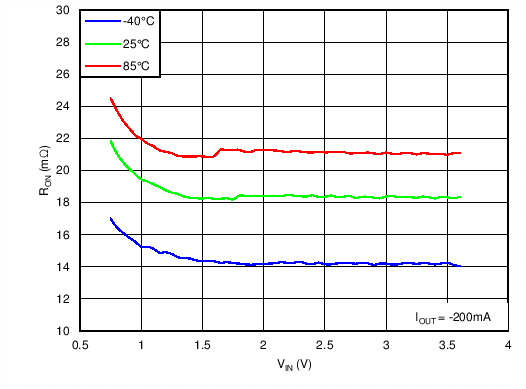 Figure 1. On-State Resistance vs Input Voltage
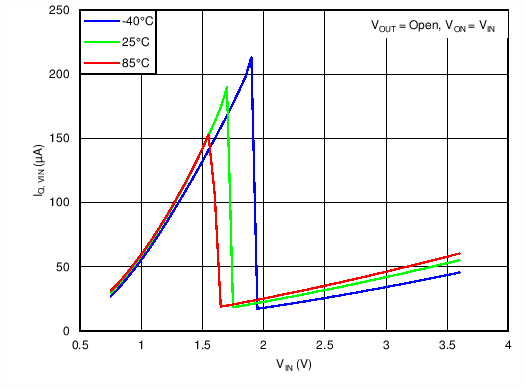 Figure 3. Quiescent Current vs Input Voltage
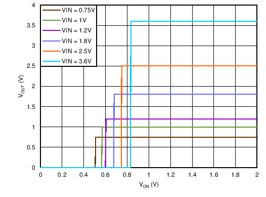 Figure 5. On Input Threshold
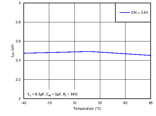 Figure 7. Turnoff Time vs Temperature
 (VIN = 3.6 V, CL = 0.1 µF, RL = 10 Ω)
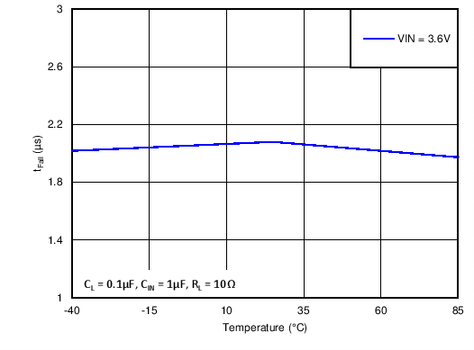 Figure 9. Fall Time vs Temperature
(VIN = 3.6 V, CL = 0.1 µF, RL = 10 Ω)
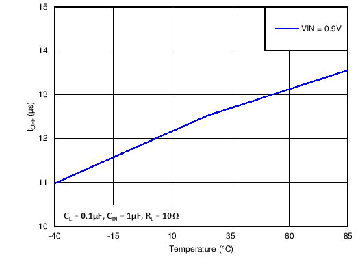 Figure 11. Turnoff Time vs Temperature
 (VIN = 0.9 V, CL = 0.1 µF, RL = 10 Ω)
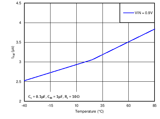 Figure 13. Fall Time vs Temperature
 (VIN = 0.9 V, CL = 0.1 µF, RL = 10 Ω)
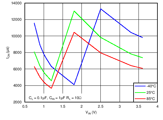 Figure 15. Turnon Time vs Input Voltage
(CL = 0.1 µF, RL = 10 Ω, VON = 1.8 V)
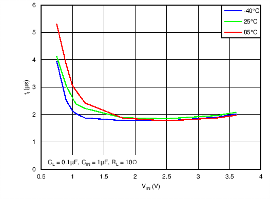 Figure 17. Fall Time vs Input Voltage
 (CL = 0.1 µF, RL = 10 Ω, VON = 1.8 V)
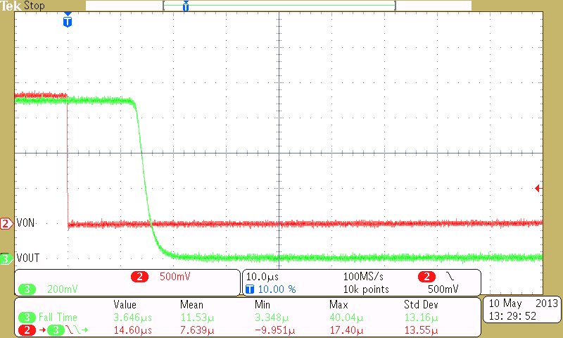 Figure 19. Turnoff Response
 (CIN = 1 µF, CL = 0.1 µF, RL = 10 Ω, VIN = 0.9 V, TA = 25°C)
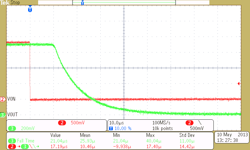 Figure 21. Turnoff Response
 (CIN = 10 µF, CL = 1 µF, RL = 10 Ω, VIN = 0.9 V, TA = 25°C)
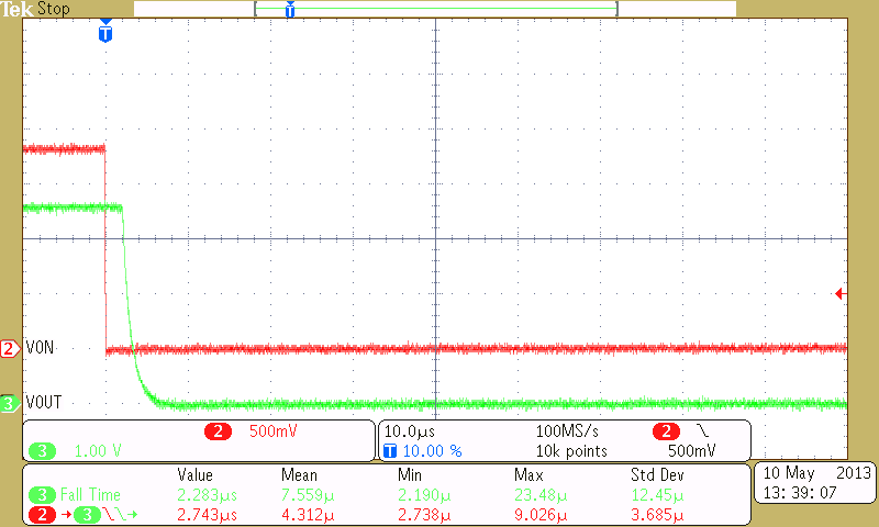 Figure 23. Turnoff Response
 (CIN = 1 µF, CL = 0.1 µF, RL = 10 Ω, VIN = 3.6 V, TA = 25°C)
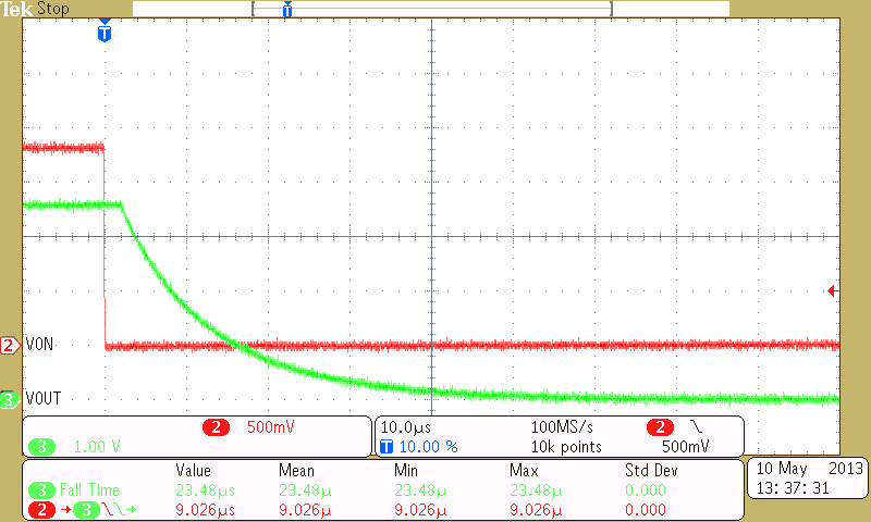 Figure 25. Turnoff Response
(CIN = 10 µF, CL = 1 µF, RL = 10 Ω, VIN = 3.6 V, TA = 25°C)
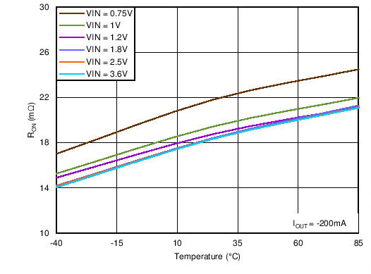 Figure 2. On-State Resistance vs Temperature
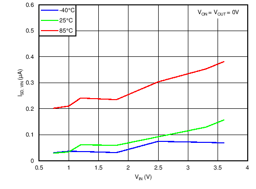 Figure 4. Shutdown Current vs Input Voltage
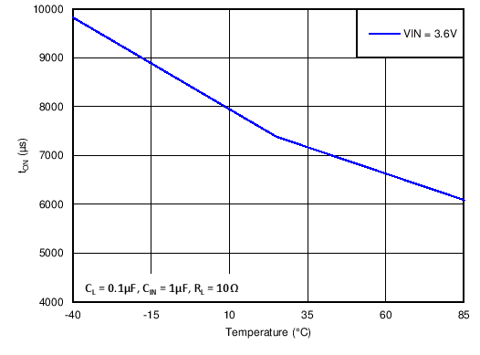 Figure 6. Turnon Time vs Temperature
 (VIN = 3.6 V, CL = 0.1 µF, RL = 10 Ω)
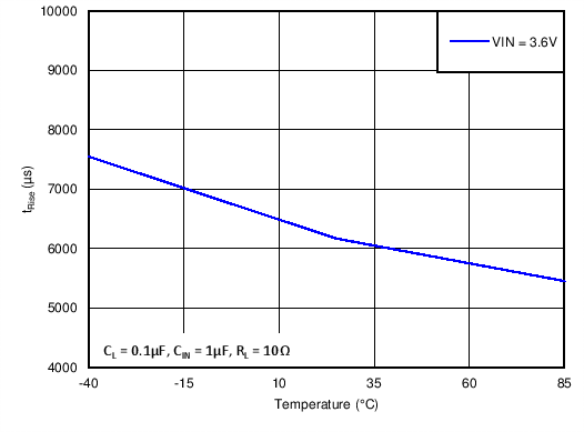 Figure 8. Rise Time vs Temperature
(VIN = 3.6 V, CL = 0.1 µF, RL = 10 Ω)
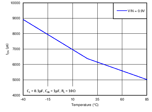 Figure 10. Turnon Time vs Temperature
 (VIN = 0.9 V, CL = 0.1 µF, RL = 10 Ω)
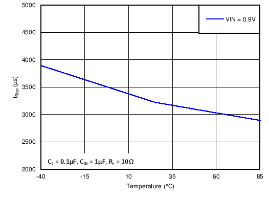 Figure 12. Rise Time vs Temperature
 (VIN = 0.9 V, CL = 0.1 µF, RL = 10 Ω)
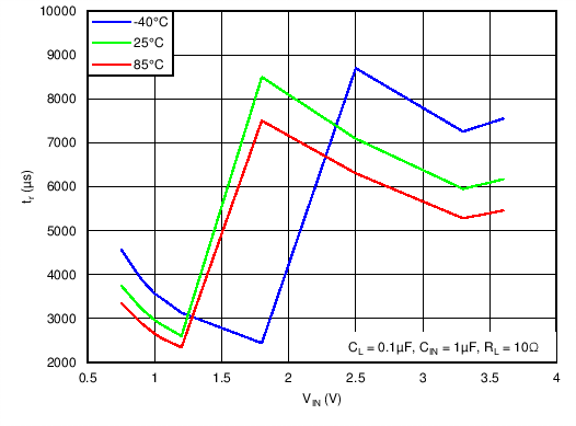 Figure 14. Rise Time vs Input Voltage
(CL = 0.1 µF, RL = 10 Ω, VON = 1.8 V)
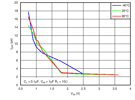 Figure 16. Turnoff Time vs Input Voltage
(CL = 0.1 µF, RL = 10 Ω, VON = 1.8 V)
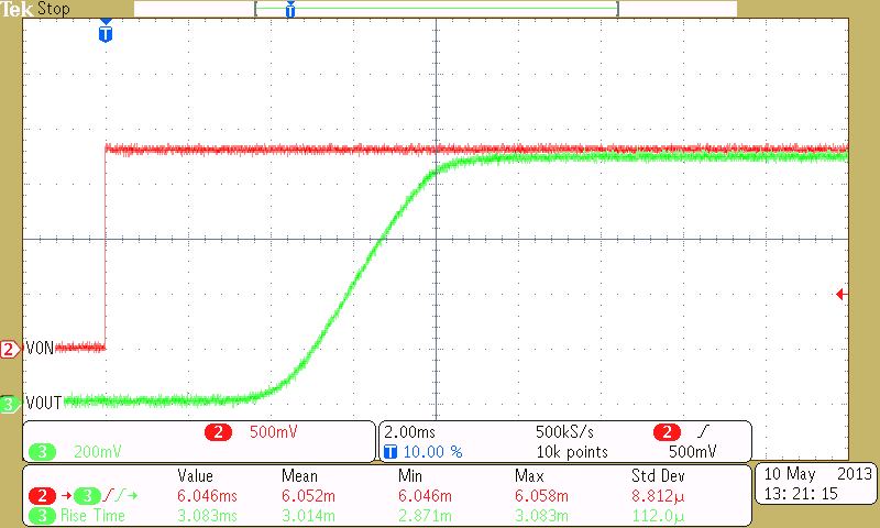
(CIN = 1 µF, CL = 0.1 µF, RL = 10 Ω, VIN = 0.9 V, TA = 25°C)
 Figure 20. Turnon Response
 (CIN = 10 µF, CL = 1 µF, RL = 10 Ω, VIN = 0.9 V, TA = 25°C)
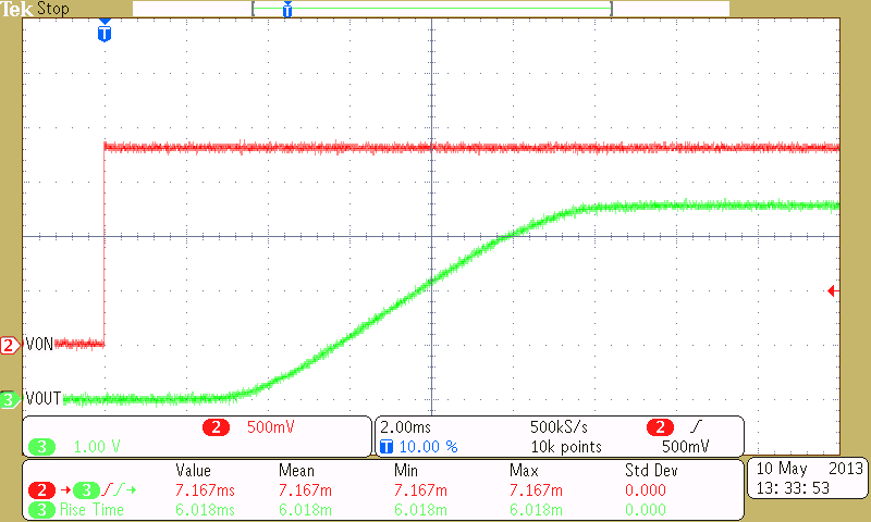 Figure 22. Turnon Response
 (CIN = 1 µF, CL = 0.1 µF, RL = 10 Ω, VIN = 3.6 V, TA = 25°C)
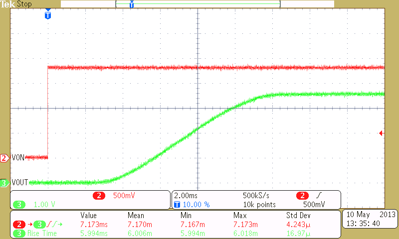 Figure 24. Turnon Response
 (CIN = 10 µF, CL = 1 µF, RL = 10 Ω, VIN = 3.6 V, TA = 25°C)