SLVSBH4F June 2012 – July 2016 TPS22966
PRODUCTION DATA.
- 1 Features
- 2 Applications
- 3 Description
- 4 Revision History
- 5 Pin Configuration and Functions
- 6 Specifications
- 7 Parameter Measurement Information
- 8 Detailed Description
- 9 Application and Implementation
- 10Power Supply Recommendations
- 11Layout
- 12Device and Documentation Support
- 13Mechanical, Packaging, and Orderable Information
Package Options
Mechanical Data (Package|Pins)
- DPU|14
Thermal pad, mechanical data (Package|Pins)
- DPU|14
Orderable Information
9 Application and Implementation
NOTE
Information in the following applications sections is not part of the TI component specification, and TI does not warrant its accuracy or completeness. TI’s customers are responsible for determining suitability of components for their purposes. Customers should validate and test their design implementation to confirm system functionality.
9.1 Application Information
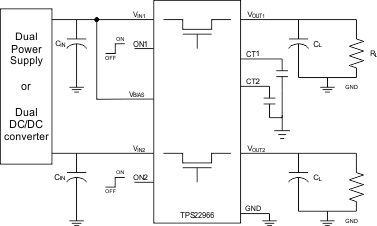
This application demonstrates how the TPS22966 can be used to limit inrush current when powering on downstream modules.
9.2 Typical Application
 Figure 33. Typical Application Circuit
9.2.1 Design Requirements
Table 2 shows the TPS22966 desgin parameters.
Table 2. Design Parameters
| DESIGN PARAMETER | VALUE |
|---|---|
| Input voltage | 3.3 V |
| Bias voltage | 5 V |
| Load capacitance (CL) | 22 µF |
| Maximum acceptable inrush current | 400 mA |
9.2.2 Detailed Design Procedure
When the switch is enabled, the output capacitors must be charged up from 0 V to the set value (3.3 V in this example). This charge arrives in the form of inrush current. Inrush current can be calculated using Equation 1.
where
- C is the output capacitance
- dV is the output voltage
- dt is the rise time
The TPS22966 offers adjustable rise time for VOUT. This feature allows the user to control the inrush current during turnon. The appropriate rise time can be calculated using Table 2 and Equation 1 as shown in Equation 2.
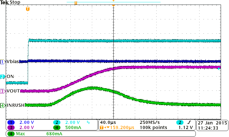
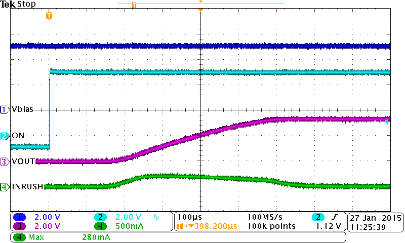
To ensure an inrush current of less than 400 mA, choose a CT value that yields a rise time of more than 181.5 μs. See the oscilloscope captures in the Application Curves section for an example of how the CT capacitor can be used to reduce inrush current.
9.2.2.1 Adjustable Rise Time
A capacitor to GND on the CTx pins sets the slew rate for each channel. To ensure desired performance, a capacitor with a minimum voltage rating of 25 V must be used on the CTx pin. An approximate formula for the relationship between CTx and slew rate is given in Equation 4. Equation 4 accounts for 10% to 90% measurement on VOUT and does NOT apply for CTx = 0 pF. (Use Table 3 to determine rise times for when CTx = 0 pF).

where
- SR is the slew rate (in µs/V)
- CT is the capacitance value on the CTx pin (in pF)
- The units for the constant 13.7 is in µs/V.
Rise time can be calculated by multiplying the input voltage by the slew rate. Table 3 shows rise time values measured on a typical device. Rise times shown in Table 3 are only valid for the power-up sequence where VIN and VBIAS are already in steady state condition, and the ON pin is asserted high.
Table 3. Rise Time Values
| CTx (pF) | RISE TIME (µs) 10% - 90%, CL = 0.1µF, CIN = 1µF, RL = 10Ω (1) |
||||||
|---|---|---|---|---|---|---|---|
| 5 V | 3.3 V | 1.8 V | 1.5 V | 1.2 V | 1.05 V | 0.8 V | |
| 0 | 124 | 88 | 63 | 60 | 53 | 49 | 42 |
| 220 | 481 | 323 | 193 | 166 | 143 | 133 | 109 |
| 470 | 855 | 603 | 348 | 299 | 251 | 228 | 175 |
| 1000 | 1724 | 1185 | 670 | 570 | 469 | 411 | 342 |
| 2200 | 3328 | 2240 | 1308 | 1088 | 893 | 808 | 650 |
| 4700 | 7459 | 4950 | 2820 | 2429 | 1920 | 1748 | 1411 |
| 10000 | 16059 | 10835 | 6040 | 5055 | 4230 | 3770 | 3033 |
9.2.3 Application Curves

| VBIAS = 5 V | VIN = 3.3 V | CL = 22 μF |

| VBIAS = 5 V | VIN = 3.3 V | CL = 22 μF |