SLUSCD1C June 2017 – November 2018 TPS2373
PRODUCTION DATA.
- 1 Features
- 2 Applications
- 3 Description
- 4 Revision History
- 5 Pin Configuration and Functions
- 6 Specifications
-
7 Detailed Description
- 7.1 Overview
- 7.2 Functional Block Diagram
- 7.3
Feature Description
- 7.3.1 APD Auxiliary Power Detect
- 7.3.2 PG Power Good (Converter Enable) Pin Interface
- 7.3.3 CLSA and CLSB Classification
- 7.3.4 DEN Detection and Enable
- 7.3.5 Internal Pass MOSFET
- 7.3.6 TPH, TPL and BT PSE Type Indicators
- 7.3.7 VC_IN, VC_OUT, UVLO_SEL, and Advanced PWM Startup
- 7.3.8 AMPS_CTL, MPS_DUTY and Automatic MPS
- 7.3.9 VDD Supply Voltage
- 7.3.10 VSS
- 7.3.11 Exposed Thermal PAD
- 7.4
Device Functional Modes
- 7.4.1 PoE Overview
- 7.4.2 Threshold Voltages
- 7.4.3 PoE Startup Sequence
- 7.4.4 Detection
- 7.4.5 Hardware Classification
- 7.4.6 Inrush and Startup
- 7.4.7 Maintain Power Signature
- 7.4.8 Advanced Startup and Converter Operation
- 7.4.9 PD Hotswap Operation
- 7.4.10 Startup and Power Management, PG and TPH, TPL, BT
- 7.4.11 Adapter ORing
- 7.4.12 Using DEN to Disable PoE
- 7.4.13 ORing Challenges
-
8 Application and Implementation
- 8.1 Application Information
- 8.2
Typical Application
- 8.2.1 Design Requirements
- 8.2.2
Detailed Design Requirements
- 8.2.2.1 Input Bridges and Schottky Diodes
- 8.2.2.2 Protection, D1
- 8.2.2.3 Capacitor, C1
- 8.2.2.4 Detection Resistor, RDEN
- 8.2.2.5 Classification Resistors, RCLSA and RCLSB
- 8.2.2.6 APD Pin Divider Network RAPD1, RAPD2
- 8.2.2.7 Opto-isolators for TPH, TPL and BT
- 8.2.2.8 VC Input and Output, CVCIN and CVCOUT
- 8.2.2.9 UVLO Select, UVLO_SEL
- 8.2.2.10 Automatic MPS and MPS Duty Cycle, RMPS and RMPS_DUTY
- 8.2.2.11 Internal Voltage Reference, RREF
- 8.2.3 Application Curves
- 9 Power Supply Recommendations
- 10Layout
- 11Device and Documentation Support
- 12Mechanical, Packaging, and Orderable Information
Package Options
Refer to the PDF data sheet for device specific package drawings
Mechanical Data (Package|Pins)
- RGW|20
Thermal pad, mechanical data (Package|Pins)
Orderable Information
7.4.8 Advanced Startup and Converter Operation
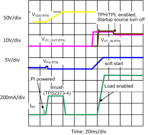
The internal PoE UVLO (Undervoltage Lock Out) circuit holds the hotswap switch off before the PSE provides full voltage to the PD. This prevents the downstream converter circuits from loading the PoE input during detection and classification. The converter circuits will discharge CBULK while the PD is unpowered. Thus V(VDD-RTN) will be a small voltage just after full voltage is applied to the PD, as seen in Figure 24. The PSE drives the PI voltage to the operating range once it has decided to power up the PD. When VVDD rises above the UVLO turn-on threshold (VUVLO_R, approximately 38 V) with RTN high, the TPS2373-3 and TPS2373-4 enables the hotswap MOSFET with inrush current limit (~200 mA for TPS2373-3 and ~335 mA for TPS2373-4) as seen in Figure 26. The PG pin is in low state while CBULK charges and VRTN falls from VVDD to nearly VVSS. VC_OUT output is also turned off during that time, providing no low supply voltage to the PWM controller,to avoid additional loading between VVDD and VRTN that could prevent successful PD and subsequent converter start up. Once the inrush current falls about 10% below the inrush current limit, the PD current limit switches to the operational level (approximately 1.85 A for TPS2373-3 and approximately 2.2 A for TPS2373-4).
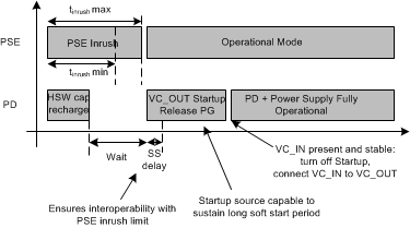
Additionally, as seen in Figure 26 once the inrush period duration has also exceeded ~81.5 ms, PG output becomes high impedance and the PWM controller startup source is turned on charging CVC_OUT, the VC_OUT capacitor, and allowing the downstream converter circuitry to start. As seen in Figure 27, the converter soft-start introduces a slight additional delay before the start of switching. Note that the startup source current capability is such that it can fully maintain VVC_OUT during the converter soft-start without requiring any significant CVC_OUT capacitance. Once VVC_IN has risen above VVCIN_ON (~8.5 V), meaning that the DC-DC converter has ramped up its output voltage, VC_IN pin is internally connected to VC_OUT pin. The startup current source is then turned off ~24 ms (tTPLHBT) later, completing the startup. TPH, TPL and BT outputs are enabled within tTPLHBT following VVC_IN rising above VVCIN_ON. If there is a fault condition preventing VVC_IN from rising during converter startup (for example a short-circuit at the output of the downstream converter), a tSTUP_OUT (~50 ms) timeout period is applied at the end of which the startup source is turned off and the VC switch is turned on, until VVC_OUT falls below VVCO_UV to initiate a new startup cycle.
The falling VC_OUT UVLO threshold (VVCO_UV) needs to be below the minimum falling UVLO threshold of the PWM controller, to ensure that every time the TPS2373 initiates a new startup cycle, the PWM controller has already reached a reset state and will initiate a new soft-start sequence. VVCO_UV is selectable between nominally 6.9 V and 3.9 V, via the UVLO_SEL input, to accommodate various PWM controllers.
 Figure 26. Power Up and Start
  Figure 27. Power Up and Start
 If VVDD-VVSS drops below the lower PoE UVLO (VUVLO_F, ~32 V), the hotswap switch is turned off, but the PG output remains high impedance allowing the converter to continue operating until VVC_OUT falls below the PWM controller's UVLO threshold. See VC Input and Output, CVCIN and CVCOUT for general guidance on how to handle PoE shutdown conditions.