SLUSCD1C June 2017 – November 2018 TPS2373
PRODUCTION DATA.
- 1 Features
- 2 Applications
- 3 Description
- 4 Revision History
- 5 Pin Configuration and Functions
- 6 Specifications
-
7 Detailed Description
- 7.1 Overview
- 7.2 Functional Block Diagram
- 7.3
Feature Description
- 7.3.1 APD Auxiliary Power Detect
- 7.3.2 PG Power Good (Converter Enable) Pin Interface
- 7.3.3 CLSA and CLSB Classification
- 7.3.4 DEN Detection and Enable
- 7.3.5 Internal Pass MOSFET
- 7.3.6 TPH, TPL and BT PSE Type Indicators
- 7.3.7 VC_IN, VC_OUT, UVLO_SEL, and Advanced PWM Startup
- 7.3.8 AMPS_CTL, MPS_DUTY and Automatic MPS
- 7.3.9 VDD Supply Voltage
- 7.3.10 VSS
- 7.3.11 Exposed Thermal PAD
- 7.4
Device Functional Modes
- 7.4.1 PoE Overview
- 7.4.2 Threshold Voltages
- 7.4.3 PoE Startup Sequence
- 7.4.4 Detection
- 7.4.5 Hardware Classification
- 7.4.6 Inrush and Startup
- 7.4.7 Maintain Power Signature
- 7.4.8 Advanced Startup and Converter Operation
- 7.4.9 PD Hotswap Operation
- 7.4.10 Startup and Power Management, PG and TPH, TPL, BT
- 7.4.11 Adapter ORing
- 7.4.12 Using DEN to Disable PoE
- 7.4.13 ORing Challenges
-
8 Application and Implementation
- 8.1 Application Information
- 8.2
Typical Application
- 8.2.1 Design Requirements
- 8.2.2
Detailed Design Requirements
- 8.2.2.1 Input Bridges and Schottky Diodes
- 8.2.2.2 Protection, D1
- 8.2.2.3 Capacitor, C1
- 8.2.2.4 Detection Resistor, RDEN
- 8.2.2.5 Classification Resistors, RCLSA and RCLSB
- 8.2.2.6 APD Pin Divider Network RAPD1, RAPD2
- 8.2.2.7 Opto-isolators for TPH, TPL and BT
- 8.2.2.8 VC Input and Output, CVCIN and CVCOUT
- 8.2.2.9 UVLO Select, UVLO_SEL
- 8.2.2.10 Automatic MPS and MPS Duty Cycle, RMPS and RMPS_DUTY
- 8.2.2.11 Internal Voltage Reference, RREF
- 8.2.3 Application Curves
- 9 Power Supply Recommendations
- 10Layout
- 11Device and Documentation Support
- 12Mechanical, Packaging, and Orderable Information
Package Options
Refer to the PDF data sheet for device specific package drawings
Mechanical Data (Package|Pins)
- RGW|20
Thermal pad, mechanical data (Package|Pins)
Orderable Information
7.4.5 Hardware Classification
Hardware classification allows a PSE to determine a PD’s power requirements before powering, and helps with power management once power is applied. Type 2, 3, and 4 hardware classification permits high power PDs to determine whether the PSE can support its high-power operation. The number of class cycles generated by the PSE prior to turn on indicates to the PD if it allots the power requested or if the allocated power is less than requested, in which case there is power demotion as shown in
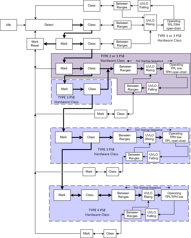
Table 3. A Type 2 PD always presents Class 4 in hardware to indicate that it is a 25.5W device. A Class 5 or 6 Type 3 PD presents Class 4 in hardware during the first two class events and it presents Class 0 or 1, respectively, for all subsequent class events. A Class 7 or 8 Type 4 PD presents Class 4 in hardware during the first two class events and it presents Class 2 or 3, respectively, for all subsequent class events. A Type 1 PSE will treat a Class 4 to 8 device like a Class 0 device, allotting 13 W if it chooses to power the PD. A Type 2 PSE will treat a Class 5 to 8 device like a Class 4 device, allotting 25.5W if it chooses to power the PD. A Class 4 PD that receives a 2-event class, a Class 5 or 6 PD that receives a 4-event class, or a Class 7 or 8 PD that receives a 5-event class, understands that the PSE has agreed to allocate the PD requested power. In the case where there is power demotion, the PD may choose to not start, or to start while not drawing more power than initially allocated, and request more power through the DLL after startup. The standard requires a Type 2, 3 or 4 PD to indicate that it is underpowered if this occurs. Startup of a high-power PD at lower power than requested implicitly requires some form of powering down sections of the application circuits.
The maximum power entries in Table 1 determine the class the PD must advertise. The PSE may disconnect a PD if it draws more than its stated class power, which may be the hardware class or a DLL-derived power level. The standard permits the PD to draw limited current peaks that increase the instantaneous power above the Table 1 limit; however, the average power requirement always applies.
The TPS2373 implements one- to five-event classification. RCLSA and RCLSB resistor values define the class of the PD. DLL communication is implemented by the Ethernet communication system in the PD and is not implemented by the TPS2373.
The TPS2373 disables classification above VCU_ON to avoid excessive power dissipation. CLSA/B voltage is turned off during PD thermal limiting or when APD or DEN is active. The CLSA and CLSB outputs are inherently current-limited, but should not be shorted to VSS for long periods of time.
Figure 25 shows how classification works for the TPS2373. Transition from state-to-state occurs when comparator thresholds are crossed (see Figure 22 and Figure 23). These comparators have hysteresis, which adds inherent memory to the machine. Operation begins at idle (unpowered by PSE) and proceeds with increasing voltage from left to right. A 2- to 5-event classification follows the (heavy lined) path towards the bottom, ending up with a latched TPL/TPH decode along the lower branch that is highlighted. Once the valid path to the PSE detection is broken, the input voltage must transition below the mark reset threshold to start anew.
 Figure 25. Up to Five-Event Class Internal States