SLVSB97E July 2012 – January 2018 TPS23751 , TPS23752
PRODUCTION DATA.
- 1 Features
- 2 Applications
- 3 Description
- 4 Revision History
- 5 Pin Configuration and Functions
-
6 Specifications
- 6.1 Absolute Maximum Ratings
- 6.2 ESD Ratings
- 6.3 ESD Ratings: Surge
- 6.4 Recommended Operating Conditions
- 6.5 Thermal Information
- 6.6 Electric Characteristics - Controller Section
- 6.7 Electrical Characteristics - Sleep Mode (TPS23752 Only)
- 6.8 Electrical Characteristics - PoE Interface Section
- 6.9 Typical Characteristics
-
7 Detailed Description
- 7.1 Overview
- 7.2 Functional Block Diagrams
- 7.3 Feature Description
- 7.4
Device Functional Modes
- 7.4.1 PoE Overview
- 7.4.2
Sleep Mode Operation (TPS23752 only)
- 7.4.2.1 Converter Controller Features
- 7.4.2.2 PWM and VFO Operation; CTL, SRT, and SRD Pin Relationships to Output Load Current
- 7.4.2.3 Bootstrap Topology
- 7.4.2.4 Current Slope Compensation and Current Limit
- 7.4.2.5 RT
- 7.4.2.6 T2P, Startup and Power Management
- 7.4.2.7 Thermal Shutdown
- 7.4.2.8 Adapter ORing
- 7.4.2.9 Using DEN to Disable PoE
- 7.4.2.10 ORing Challenges
-
8 Application and Implementation
- 8.1 Application Information
- 8.2
Typical Application
- 8.2.1 Design Requirements
- 8.2.2
Detailed Design Procedure
- 8.2.2.1 Input Bridges and Schottky Diodes
- 8.2.2.2 Protection, D1
- 8.2.2.3 Capacitor, C1
- 8.2.2.4 Detection Resistor, RDEN
- 8.2.2.5 Classification Resistor, RCLS
- 8.2.2.6 APD Pin Divider Network, RAPD1, RAPD2
- 8.2.2.7 Setting the PWM-VFO Threshold using the SRT pin
- 8.2.2.8 Setting Frequency (RT)
- 8.2.2.9 Current Slope Compensation
- 8.2.2.10 Voltage Feed-Forward Compensation
- 8.2.2.11 Estimating Bias Supply Requirements and Cvc
- 8.2.2.12 Switching Transformer Considerations and RVC
- 8.2.2.13 T2P Pin Interface
- 8.2.2.14 Softstart
- 8.2.2.15 Special Switching MOSFET Considerations
- 8.2.2.16 ESD
- 8.2.2.17 Thermal Considerations and OTSD
- 8.2.3 Application Curves
- 9 Power Supply Recommendations
- 10Layout
- 11Device and Documentation Support
- 12Mechanical, Packaging, and Orderable Information
Package Options
Mechanical Data (Package|Pins)
- PWP|16
Thermal pad, mechanical data (Package|Pins)
- PWP|16
Orderable Information
7.4.1.8 PD Hotswap Operation
IEEE 802.3at has taken a new approach to PSE output limiting. A type 2 PSE must meet an output current versus time template with specified minimum and maximum sourcing boundaries. The peak output current may be as high as 50 A for 10 μs or 1.75 A for 75 ms. This makes robust protection of the PD device even more important than it was in IEEE 802.3-2008.
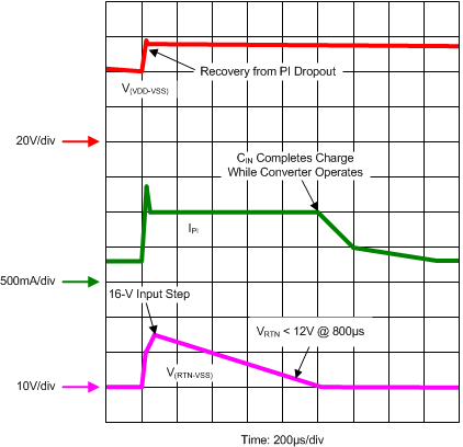
The internal hotswap MOSFET is protected against output faults and input voltage steps with a current limit and deglitched (time-delay filtered) foldback. An overload on the pass MOSFET engages the current limit, with VRTN-VVSS rising as a result. If VRTN rises above approximately 12 V for longer than approximately 800 μs, the current limit reverts to the inrush value, and turns the converter off. The 800 μs deglitch feature prevents momentary transients from causing a PD reset, provided that recovery lies within the bounds of the hotswap and PSE protection. Figure 27 shows an example of recovery from a 16 V PSE rising voltage step. The hotswap MOSFET goes into current limit, overshooting to a relatively low current, recovers to approximately 1000 mA full current limit and charges the input capacitor while the converter continues to run. The MOSFET did not go into foldback because VRTN-VVSS was below 12 V after the 800 μs deglitch.
 Figure 27. Response to Output Short Circuit
The PD control has a thermal sensor that protects the internal hotswap MOSFET. Conditions like startup or operation into a VDD-to-RTN short cause high power dissipation in the MOSFET. An over-temperature shutdown (OTSD) turns off the hotswap MOSFET and class regulator, which are restarted after the device cools. The hotswap MOSFET is re-enabled with the inrush current limit when exiting from an over-temperature event.
Pulling DEN to VSS during powered operation causes the internal hotswap MOSFET to turn off. The hotswap switch is forced off under the following conditions:
- VAPD above VAPDEN (approximately 1.5 V)
- V(DEN –VSS) < VPD_DIS when VVDD– VVSS is in the operational range,
- PD OTSD is active, or
- V(DEN –VSS) < PoE UVLO falling threshold (approximately 32 V).