SLVSB97E July 2012 – January 2018 TPS23751 , TPS23752
PRODUCTION DATA.
- 1 Features
- 2 Applications
- 3 Description
- 4 Revision History
- 5 Pin Configuration and Functions
-
6 Specifications
- 6.1 Absolute Maximum Ratings
- 6.2 ESD Ratings
- 6.3 ESD Ratings: Surge
- 6.4 Recommended Operating Conditions
- 6.5 Thermal Information
- 6.6 Electric Characteristics - Controller Section
- 6.7 Electrical Characteristics - Sleep Mode (TPS23752 Only)
- 6.8 Electrical Characteristics - PoE Interface Section
- 6.9 Typical Characteristics
-
7 Detailed Description
- 7.1 Overview
- 7.2 Functional Block Diagrams
- 7.3 Feature Description
- 7.4
Device Functional Modes
- 7.4.1 PoE Overview
- 7.4.2
Sleep Mode Operation (TPS23752 only)
- 7.4.2.1 Converter Controller Features
- 7.4.2.2 PWM and VFO Operation; CTL, SRT, and SRD Pin Relationships to Output Load Current
- 7.4.2.3 Bootstrap Topology
- 7.4.2.4 Current Slope Compensation and Current Limit
- 7.4.2.5 RT
- 7.4.2.6 T2P, Startup and Power Management
- 7.4.2.7 Thermal Shutdown
- 7.4.2.8 Adapter ORing
- 7.4.2.9 Using DEN to Disable PoE
- 7.4.2.10 ORing Challenges
-
8 Application and Implementation
- 8.1 Application Information
- 8.2
Typical Application
- 8.2.1 Design Requirements
- 8.2.2
Detailed Design Procedure
- 8.2.2.1 Input Bridges and Schottky Diodes
- 8.2.2.2 Protection, D1
- 8.2.2.3 Capacitor, C1
- 8.2.2.4 Detection Resistor, RDEN
- 8.2.2.5 Classification Resistor, RCLS
- 8.2.2.6 APD Pin Divider Network, RAPD1, RAPD2
- 8.2.2.7 Setting the PWM-VFO Threshold using the SRT pin
- 8.2.2.8 Setting Frequency (RT)
- 8.2.2.9 Current Slope Compensation
- 8.2.2.10 Voltage Feed-Forward Compensation
- 8.2.2.11 Estimating Bias Supply Requirements and Cvc
- 8.2.2.12 Switching Transformer Considerations and RVC
- 8.2.2.13 T2P Pin Interface
- 8.2.2.14 Softstart
- 8.2.2.15 Special Switching MOSFET Considerations
- 8.2.2.16 ESD
- 8.2.2.17 Thermal Considerations and OTSD
- 8.2.3 Application Curves
- 9 Power Supply Recommendations
- 10Layout
- 11Device and Documentation Support
- 12Mechanical, Packaging, and Orderable Information
Package Options
Mechanical Data (Package|Pins)
- PWP|16
Thermal pad, mechanical data (Package|Pins)
- PWP|16
Orderable Information
8.2.2.14 Softstart
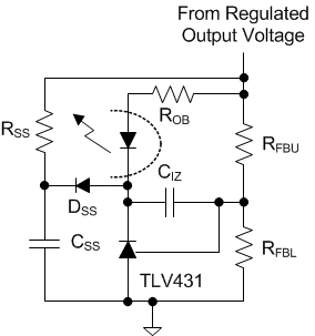
Converters require a softstart on the voltage error amplifier to prevent output overshoot on startup. Figure 35 shows a common implementation of a secondary-side softstart that works with the typical TL431 error amplifier. The softstart components consist of DSS, RSS, and CSS. They serve to control the output rate-of-rise by pulling VCTL down as CSS charges through ROB, the optocoupler, and DSS. This has the added advantage that the TL431 output and CIZ are preset to the proper value as the output voltage reaches the regulated value, preventing voltage overshoot due to the error amplifier recovery. The secondary-side error amplifier does not become active until there is sufficient voltage on the secondary. The TPS23751 and TPS23752 provide a primary-side softstart which persists long enough (approximately 3ms) for secondary side voltage-loop softstart to take over. The primary-side current-loop softstart controls the switching MOSFET peak current by applying a slowly rising ramp voltage to a second PWM control input. The PWM is controlled by the lower of the softstart ramp or the CTL-derived current demand. The actual output voltage rise time is usually much shorter than the internal softstart period. Initially the internal softstart ramp limits the maximum current demand as a function of time. The current limit, secondary-side softstart, or output regulation assume control of the PWM before the internal softstart period is over.
 Figure 35. Error Amplifier Soft Start