SLVSB97E July 2012 – January 2018 TPS23751 , TPS23752
PRODUCTION DATA.
- 1 Features
- 2 Applications
- 3 Description
- 4 Revision History
- 5 Pin Configuration and Functions
-
6 Specifications
- 6.1 Absolute Maximum Ratings
- 6.2 ESD Ratings
- 6.3 ESD Ratings: Surge
- 6.4 Recommended Operating Conditions
- 6.5 Thermal Information
- 6.6 Electric Characteristics - Controller Section
- 6.7 Electrical Characteristics - Sleep Mode (TPS23752 Only)
- 6.8 Electrical Characteristics - PoE Interface Section
- 6.9 Typical Characteristics
-
7 Detailed Description
- 7.1 Overview
- 7.2 Functional Block Diagrams
- 7.3 Feature Description
- 7.4
Device Functional Modes
- 7.4.1 PoE Overview
- 7.4.2
Sleep Mode Operation (TPS23752 only)
- 7.4.2.1 Converter Controller Features
- 7.4.2.2 PWM and VFO Operation; CTL, SRT, and SRD Pin Relationships to Output Load Current
- 7.4.2.3 Bootstrap Topology
- 7.4.2.4 Current Slope Compensation and Current Limit
- 7.4.2.5 RT
- 7.4.2.6 T2P, Startup and Power Management
- 7.4.2.7 Thermal Shutdown
- 7.4.2.8 Adapter ORing
- 7.4.2.9 Using DEN to Disable PoE
- 7.4.2.10 ORing Challenges
-
8 Application and Implementation
- 8.1 Application Information
- 8.2
Typical Application
- 8.2.1 Design Requirements
- 8.2.2
Detailed Design Procedure
- 8.2.2.1 Input Bridges and Schottky Diodes
- 8.2.2.2 Protection, D1
- 8.2.2.3 Capacitor, C1
- 8.2.2.4 Detection Resistor, RDEN
- 8.2.2.5 Classification Resistor, RCLS
- 8.2.2.6 APD Pin Divider Network, RAPD1, RAPD2
- 8.2.2.7 Setting the PWM-VFO Threshold using the SRT pin
- 8.2.2.8 Setting Frequency (RT)
- 8.2.2.9 Current Slope Compensation
- 8.2.2.10 Voltage Feed-Forward Compensation
- 8.2.2.11 Estimating Bias Supply Requirements and Cvc
- 8.2.2.12 Switching Transformer Considerations and RVC
- 8.2.2.13 T2P Pin Interface
- 8.2.2.14 Softstart
- 8.2.2.15 Special Switching MOSFET Considerations
- 8.2.2.16 ESD
- 8.2.2.17 Thermal Considerations and OTSD
- 8.2.3 Application Curves
- 9 Power Supply Recommendations
- 10Layout
- 11Device and Documentation Support
- 12Mechanical, Packaging, and Orderable Information
Package Options
Mechanical Data (Package|Pins)
- PWP|20
Thermal pad, mechanical data (Package|Pins)
- PWP|20
Orderable Information
8.2 Typical Application
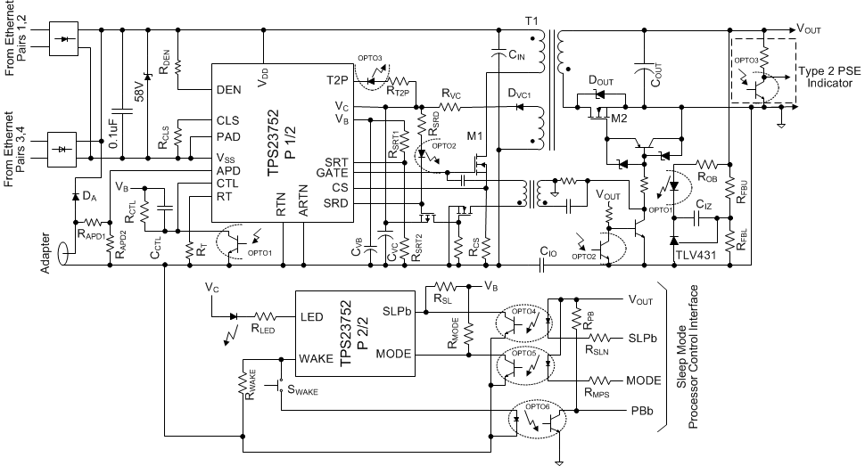
 Figure 31. TPS23752 Application Circuit