SLVS728D January 2007 – October 2019 TPS2412 , TPS2413
PRODUCTION DATA.
- 1 Features
- 2 Applications
- 3 Description
- 4 Revision History
- 5 Device Comparison Table
- 6 Pin Configuration and Functions
- 7 Specifications
-
8 Detailed Description
- 8.1 Overview
- 8.2 Functional Block Diagram
- 8.3
Feature Description
- 8.3.1 Definitions
- 8.3.2 TPS2412 vs TPS2413 – MOSFET Control Methods
- 8.3.3 N+1 Power Supply – Typical Connection
- 8.3.4 Input ORing – Typical Connection
- 8.3.5 System Design and Behavior With Transients
- 8.3.6 TPS2412 Regulation-Loop Stability
- 8.3.7 MOSFET Selection and R(RSET)
- 8.3.8 Gate Drive, Charge Pump and C(BYP)
- 8.4 Device Functional Modes
- 9 Application and Implementation
- 10Power Supply Recommendations
- 11Layout
- 12Device and Documentation Support
- 13Mechanical, Packaging, and Orderable Information
Package Options
Refer to the PDF data sheet for device specific package drawings
Mechanical Data (Package|Pins)
- D|8
- PW|8
Thermal pad, mechanical data (Package|Pins)
Orderable Information
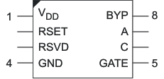
6 Pin Configuration and Functions
PW and D Packages
8-Pins TSSOP and SOIC
Top View

Pin Functions
| PIN | I/O | DESCRIPTION | |
|---|---|---|---|
| NAME | NO. | ||
| VDD | 1 | PWR | Input power for the gate drive charge pump and internal controls. VDD must be connected to a supply voltage ≥ 3 V. |
| RSET | 2 | I | Connect a resistor to ground to program the turnoff threshold. Leaving RSET open results in a slightly positive V(A-C) turnoff threshold. |
| RSVD | 3 | PWR | This pin must be connected to GND. |
| GND | 4 | PWR | Device ground. |
| GATE | 5 | O | Connect to the gate of the external MOSFET. Controls the MOSFET to emulate a low forward-voltage diode. |
| C | 6 | I | Voltage sense input that connects to the simulated diode cathode. Connect to the MOSFET drain in the typical configuration. |
| A | 7 | I | Voltage sense input that connects to the simulated diode anode. A also serves as the reference for the charge-pump bias supply on BYP. Connect to the MOSFET source in the typical configuration. |
| BYP | 8 | I/O | Connect a storage capacitor from BYP to A to filter the gate drive supply voltage. |