SLVSC87C October 2013 – December 2018 TPS24750 , TPS24751
UNLESS OTHERWISE NOTED, this document contains PRODUCTION DATA.
- 1 Features
- 2 Applications
- 3 Description
- 4 Revision History
- 5 Device Comparison Table
- 6 Pin Configuration and Functions
- 7 Specifications
- 8 Parameter Measurement Information
-
9 Detailed Descriptions
- 9.1 Overview
- 9.2 Functional Block Diagram
- 9.3 Feature Description
- 9.4 Device Functional Modes
-
10Application and Implementation
- 10.1 Application Information
- 10.2
Typical Application
- 10.2.1 Design Requirements
- 10.2.2
Detailed Design Procedure
- 10.2.2.1
Power-Limited Start-Up
- 10.2.2.1.1 STEP 1. Choose RSENSE, RSET, and RIMON
- 10.2.2.1.2 STEP 2. Choose Power-Limit Value, PLIM, and RPROG
- 10.2.2.1.3 STEP 3. Choose Output Voltage Rising Time, tON, and Timing Capacitor CT
- 10.2.2.1.4 STEP 4. Calculate the Retry-Mode Duty Ratio
- 10.2.2.1.5 STEP 5. Select R1, R2, and R3 for UV and OV
- 10.2.2.1.6 STEP 6. Choose R4, R5, and C1
- 10.2.2.2 Alternative Design Example: Gate Capacitor (dv/dt) Control in Inrush Mode
- 10.2.2.3 Additional Design Considerations
- 10.2.2.1
Power-Limited Start-Up
- 10.2.3 Application Curves
- 10.3 System Examples
- 11Power Supply Recommendations
- 12Layout
- 13Device and Documentation Support
- 14Mechanical, Packaging, and Orderable Information
Package Options
Mechanical Data (Package|Pins)
- RUV|36
Thermal pad, mechanical data (Package|Pins)
- RUV|36
Orderable Information
9.4.3 Action of the Constant-Power Engine
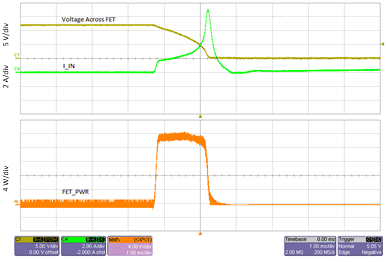
Figure 32 illustrates the operation of the constant-power engine during start-up. The circuit used to generate the waveforms of Figure 32 was programmed to a power limit of 21 W by means of the resistor connected between PROG and GND. At the moment current begins to flow through the internal FET, a voltage of 12 V appears across it (input voltage VVCC = 12 V), and the constant-power engine therefore allows a current of 1.75 A (equal to 21 W divided by 12 V) to flow. This current increases in inverse ratio as the drain-to-source voltage diminishes, so as to maintain a constant dissipation of 21 W. The constant-power engine adjusts the current by altering the reference signal fed to the current limit amplifier. The lower part of Figure 32 shows the measured power dissipated in the internal FET, labeled FET PWR, remaining substantially constant during this period of operation, which ends when the current through the FET reaches the current limit ILIM. This behavior can be considered a form of foldback limiting, but unlike the standard linear form of foldback limiting, it allows the power device to operate near its maximum capability, thus reducing the start-up time.
 Figure 32. Computation of Power Stress During Startup