SLVSC87C October   2013  – December 2018 TPS24750 , TPS24751

UNLESS OTHERWISE NOTED, this document contains PRODUCTION DATA.  

  1. Features
  2. Applications
  3. Description
    1.     Device Images
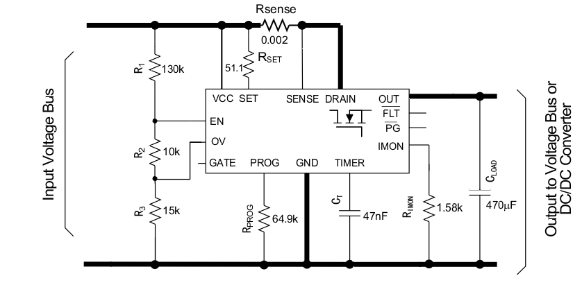
      1.      Application Schematic (12 V at 10 A)
      2.      Transient Output Short Circuit Response
  4. Revision History
  5. Device Comparison Table
  6. Pin Configuration and Functions
    1.     Pin Functions
  7. Specifications
    1. 7.1 Absolute Maximum Ratings
    2. 7.2 ESD Ratings
    3. 7.3 Recommended Operating Conditions
    4. 7.4 Thermal Information
    5. 7.5 Electrical Characteristics
    6. 7.6 Typical Characteristics
  8. Parameter Measurement Information
  9. Detailed Descriptions
    1. 9.1 Overview
    2. 9.2 Functional Block Diagram
    3. 9.3 Feature Description
      1. 9.3.1  DRAIN
      2. 9.3.2  EN
      3. 9.3.3  FLTb
      4. 9.3.4  GATE
      5. 9.3.5  GND
      6. 9.3.6  IMON
      7. 9.3.7  OUT
      8. 9.3.8  OV
      9. 9.3.9  PGb
      10. 9.3.10 PROG
      11. 9.3.11 SENSE
      12. 9.3.12 TIMER
      13. 9.3.13 VCC
    4. 9.4 Device Functional Modes
      1. 9.4.1 Board Plug-In
      2. 9.4.2 Inrush Operation
      3. 9.4.3 Action of the Constant-Power Engine
      4. 9.4.4 Circuit Breaker and Fast Trip
      5. 9.4.5 Automatic Restart
      6. 9.4.6 Start-Up with Short on Output
      7. 9.4.7 PGb, FLTb, and Timer Operations
        1. 9.4.7.1 Overtemperature Shutdown
        2. 9.4.7.2 Start-Up of Hot-Swap Circuit by VCC or EN
  10. 10Application and Implementation
    1. 10.1 Application Information
    2. 10.2 Typical Application
      1. 10.2.1 Design Requirements
      2. 10.2.2 Detailed Design Procedure
        1. 10.2.2.1 Power-Limited Start-Up
          1. 10.2.2.1.1 STEP 1. Choose RSENSE, RSET, and RIMON
          2. 10.2.2.1.2 STEP 2. Choose Power-Limit Value, PLIM, and RPROG
          3. 10.2.2.1.3 STEP 3. Choose Output Voltage Rising Time, tON, and Timing Capacitor CT
          4. 10.2.2.1.4 STEP 4. Calculate the Retry-Mode Duty Ratio
          5. 10.2.2.1.5 STEP 5. Select R1, R2, and R3 for UV and OV
          6. 10.2.2.1.6 STEP 6. Choose R4, R5, and C1
        2. 10.2.2.2 Alternative Design Example: Gate Capacitor (dv/dt) Control in Inrush Mode
        3. 10.2.2.3 Additional Design Considerations
          1. 10.2.2.3.1 Use of PGb
          2. 10.2.2.3.2 Output Clamp Diode
          3. 10.2.2.3.3 Gate Clamp Diode
          4. 10.2.2.3.4 Bypass Capacitors
          5. 10.2.2.3.5 Output Short-Circuit Measurements
      3. 10.2.3 Application Curves
    3. 10.3 System Examples
  11. 11Power Supply Recommendations
    1. 11.1 Transient Thermal Impedance
  12. 12Layout
    1. 12.1 Layout Guidelines
    2. 12.2 Layout Example
  13. 13Device and Documentation Support
    1. 13.1 Documentation Support
      1. 13.1.1 Related Documentation
    2. 13.2 Related Links
    3. 13.3 Receiving Notification of Documentation Updates
    4. 13.4 Community Resources
    5. 13.5 Trademarks
    6. 13.6 Electrostatic Discharge Caution
    7. 13.7 Export Control Notice
    8. 13.8 Glossary
  14. 14Mechanical, Packaging, and Orderable Information

Package Options

Mechanical Data (Package|Pins)
Thermal pad, mechanical data (Package|Pins)
Orderable Information

Device Images

Application Schematic (12 V at 10 A)

TPS24750 TPS24751 typ_app_FP_slvsc87.gif

Transient Output Short Circuit Response

TPS24750 TPS24751 C3000_slvsc87.gif