SLVS503F November 2003 – February 2020 TPS2490 , TPS2491
PRODUCTION DATA.
- 1 Features
- 2 Applications
- 3 Description
- 4 Revision History
- 5 Pin Configuration and Functions
- 6 Specifications
- 7 Detailed Description
- 8 Application and Implementation
- 9 Power Supply Recommendations
- 10Layout
- 11Device and Documentation Support
- 12Mechanical, Packaging, and Orderable Information
Package Options
Refer to the PDF data sheet for device specific package drawings
Mechanical Data (Package|Pins)
- DGS|10
Thermal pad, mechanical data (Package|Pins)
Orderable Information
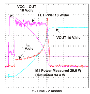
7.4.3 Action of the Constant Power Engine (Figure 14)
The calculated power dissipated in Q1, VDS ×ID, is computed under the same startup conditions as Figure 13 . The current of Q1, labeled IIN, initially rises to the value that satisfies the constant power engine; in this case it is
34 W ÷ 48 V = 0.7 A. The 34 W value is programmed into the engine by setting the PROG voltage using Equation 2 given in the PROG. VDS of Q1, which is calculated as V(SENSE–OUT), falls as CO charges, thus allowing the Q1 drain current to increase. This is the result of the internal constant power engine adjusting the current limit reference to the GATE amplifier as CO charges and VDS falls. The calculated device power in Figure 14, labeled FET PWR, is seen to be flat-topped and constant within the limitations of circuit tolerance and acquisition noise. A fixed current limit is implemented by clamping the constant power engine’s output to 50 mV when VDS is low. This protection technique can be viewed as a specialized form of foldback limiting; the benefit over linear foldback is that it yields the maximum output current from a device over the full range of VDS and still protects the device.
 Figure 14. Computation of Q1 Stress During Startup