SLVSCC8A May 2014 – December 2014 TPS2513A-Q1 , TPS2514A-Q1
PRODUCTION DATA.
- 1 Features
- 2 Applications
- 3 Description
- 4 Revision History
- 5 Pin Configuration and Functions
- 6 Specifications
- 7 Detailed Description
- 8 Applications and Implementation
- 9 Power Supply Recommendations
- 10Layout
- 11Device and Documentation Support
Package Options
Mechanical Data (Package|Pins)
- DBV|6
Thermal pad, mechanical data (Package|Pins)
Orderable Information
1 Features
- AEC-Q100 Qualified:
- Automatically Selects Charge Mode
- D+ and D- Divider Mode 2.7 V and 2.7 V
- D+ and D- 1.2 V Mode
- D+ and D- Shorted Mode per USB Battery Charging Specification, Revision 1.2 (BC1.2)
- Operating Range: 4.5 V to 5.5 V
- Dual USB Charging Port Controller,
TPS2513A-Q1 - Single USB Charging Port Controller,
TPS2514A-Q1 - Available in SOT23-6 Package
2 Applications
- Automotive USB Power Charger
- Car Charger
3 Description
The TPS2513A-Q1 and TPS2514A-Q1 are USB dedicated charging port (DCP) controllers, used for the charging of most popular mobile phones and tablets. An auto-detect feature monitors USB data line voltage, and automatically provides the correct electrical signatures on the data lines to charge compliant devices among the following dedicated charging schemes:
- Divider 3 mode, required to apply 2.7 V and 2.7 V on the D+ and D- Lines respectively
- BC1.2 shorted mode, required to short the D+ Line to the D– Line
- 1.2 V mode, required to apply 1.2 V on the D+ and D- Lines
Use with the TPS2561A-Q1 and TPS2513A-Q1 (dual channel), TPS2557-Q1 and TPS2514A-Q1 (single channel) for low loss, automotive qualified, USB Charging Port Solution capable of charging all of today's popular phones and tablets.
Device Information (1)
| PART NUMBER | PACKAGE | BODY SIZE (NOM) |
|---|---|---|
| TPS2513A-Q1 | SOT-23 (6) | 2.90mm x 1.60mm |
| TPS2514A-Q1 |
- For all available packages, see the orderable addendum at the end of the datasheet.
Simplified Application Diagram
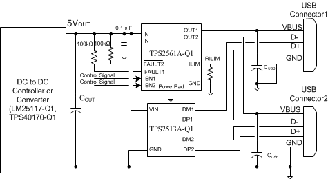
Typical Application as USB Dedicated Charging Port Controller of Dual Port Automotive USB Charge Port Solution