SLVS736C February   2008  – October 2023 TPS2550 , TPS2551

PRODUCTION DATA  

  1.   1
  2. Features
  3. Applications
  4. Description
  5. Revision History
  6. Device Comparison Table
  7. Pin Configuration and Functions
  8. Specifications
    1. 7.1 Absolute Maximum Ratings
    2. 7.2 ESD Ratings
    3. 7.3 Recommended Operating Conditions
    4. 7.4 Thermal Information
    5. 7.5 Electrical Characteristics
    6. 7.6 Typical Characteristics
  9. Parameter Measurement Information
  10. Detailed Description
    1. 9.1 Overview
    2. 9.2 Functional Block Diagram
    3. 9.3 Feature Description
      1. 9.3.1 Overcurrent
      2. 9.3.2 Reverse-Voltage Protection
      3. 9.3.3 FAULT Response
      4. 9.3.4 Undervoltage Lockout (UVLO)
      5. 9.3.5 ENABLE ( EN or EN)
      6. 9.3.6 Thermal Sense
      7. 9.3.7 Device Functional Modes
    4. 9.4 Programming
      1. 9.4.1 Programming the Current-Limit Threshold
  11. 10Application and Implementation
    1. 10.1 Application Information
    2. 10.2 Typical Applications
      1. 10.2.1 Two-Level Current-Limit Circuit
      2. 10.2.2 Design Requirements
      3. 10.2.3 Detail Design Procedures
        1. 10.2.3.1 Designing Above a Minimum Current Limit
        2. 10.2.3.2 Designing Below a Maximum Current Limit
        3. 10.2.3.3 Input and Output Capacitance
      4. 10.2.4 Auto-Retry Functionality
      5. 10.2.5 Latch-Off Functionality
      6. 10.2.6 Typical Application as USB Power Switch
        1. 10.2.6.1 Design Requirements
          1. 10.2.6.1.1 USB Power-Distribution Requirements
        2. 10.2.6.2 Detail Design Procedures
          1. 10.2.6.2.1 Universal Serial Bus (USB) Power-Distribution Requirements
    3. 10.3 Power Supply Recommendations
      1. 10.3.1 Self-Powered and Bus-Powered Hubs
      2. 10.3.2 Low-Power Bus-Powered and High-Power Bus-Powered Functions
      3. 10.3.3 Power Dissipation and Junction Temperature
    4. 10.4 Layout
      1. 10.4.1 Layout Guidelines
      2. 10.4.2 Layout Example
  12. 11Device and Documentation Support
    1. 11.1 Receiving Notification of Documentation Updates
    2. 11.2 Support Resources
    3. 11.3 Trademarks
    4. 11.4 Electrostatic Discharge Caution
    5. 11.5 Glossary
  13. 12Mechanical, Packaging, and Orderable Information

Package Options

Mechanical Data (Package|Pins)
Thermal pad, mechanical data (Package|Pins)
Orderable Information

Description

The TPS2550/51 power-distribution switch is intended for applications where heavy capacitive loads and short-circuits are likely to be encountered, incorporating a 100-mΩ, N-channel MOSFET in a single package. The current-limit threshold is user adjustable between 100 mA and 1.1 A via an external resistor. The power-switch rise and fall times are controlled to minimize current surges during switching.

The device limits the output current to a desired level by switching into a constant-current mode when the output load exceeds the current-limit threshold or a short is present. An internal reverse-voltage detection comparator disables the power-switch in the event that the output voltage is driven higher than the input to protect devices on the input side of the switch. The FAULT logic output asserts low during both overcurrent and reverse-voltage conditions.

Package Information
PART NUMBER PACKAGE(1) BODY SIZE (NOM)
TPS255x SOT-23 (6) 2.90 mm × 1.60 mm
WSON (6) 2.00 mm × 2.00 mm
For all available packages, see the orderable addendum at the end of the data sheet.
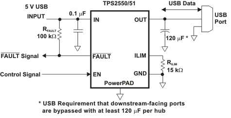
GUID-DB53490B-1D5D-419D-A5CB-74B966FC7F88-low.gif Figure 3-1 Typical Application as USB Power Switch