SLVS736C February   2008  – October 2023 TPS2550 , TPS2551

PRODUCTION DATA  

  1.   1
  2. Features
  3. Applications
  4. Description
  5. Revision History
  6. Device Comparison Table
  7. Pin Configuration and Functions
  8. Specifications
    1. 7.1 Absolute Maximum Ratings
    2. 7.2 ESD Ratings
    3. 7.3 Recommended Operating Conditions
    4. 7.4 Thermal Information
    5. 7.5 Electrical Characteristics
    6. 7.6 Typical Characteristics
  9. Parameter Measurement Information
  10. Detailed Description
    1. 9.1 Overview
    2. 9.2 Functional Block Diagram
    3. 9.3 Feature Description
      1. 9.3.1 Overcurrent
      2. 9.3.2 Reverse-Voltage Protection
      3. 9.3.3 FAULT Response
      4. 9.3.4 Undervoltage Lockout (UVLO)
      5. 9.3.5 ENABLE ( EN or EN)
      6. 9.3.6 Thermal Sense
      7. 9.3.7 Device Functional Modes
    4. 9.4 Programming
      1. 9.4.1 Programming the Current-Limit Threshold
  11. 10Application and Implementation
    1. 10.1 Application Information
    2. 10.2 Typical Applications
      1. 10.2.1 Two-Level Current-Limit Circuit
      2. 10.2.2 Design Requirements
      3. 10.2.3 Detail Design Procedures
        1. 10.2.3.1 Designing Above a Minimum Current Limit
        2. 10.2.3.2 Designing Below a Maximum Current Limit
        3. 10.2.3.3 Input and Output Capacitance
      4. 10.2.4 Auto-Retry Functionality
      5. 10.2.5 Latch-Off Functionality
      6. 10.2.6 Typical Application as USB Power Switch
        1. 10.2.6.1 Design Requirements
          1. 10.2.6.1.1 USB Power-Distribution Requirements
        2. 10.2.6.2 Detail Design Procedures
          1. 10.2.6.2.1 Universal Serial Bus (USB) Power-Distribution Requirements
    3. 10.3 Power Supply Recommendations
      1. 10.3.1 Self-Powered and Bus-Powered Hubs
      2. 10.3.2 Low-Power Bus-Powered and High-Power Bus-Powered Functions
      3. 10.3.3 Power Dissipation and Junction Temperature
    4. 10.4 Layout
      1. 10.4.1 Layout Guidelines
      2. 10.4.2 Layout Example
  12. 11Device and Documentation Support
    1. 11.1 Receiving Notification of Documentation Updates
    2. 11.2 Support Resources
    3. 11.3 Trademarks
    4. 11.4 Electrostatic Discharge Caution
    5. 11.5 Glossary
  13. 12Mechanical, Packaging, and Orderable Information

Package Options

Mechanical Data (Package|Pins)
Thermal pad, mechanical data (Package|Pins)
Orderable Information

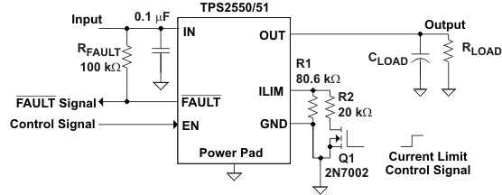
Two-Level Current-Limit Circuit

Some applications require different current-limit thresholds depending on external system conditions. Figure 10-5 shows an implementation for an externally controlled, two-level current-limit circuit. The current-limit threshold is set by the total resistance from ILIM to GND (see previously discussed "Programming the Current-Limit Threshold" section). A logic-level input enables/disables MOSFET Q1 and changes the current-limit threshold by modifying the total resistance from ILIM to GND. Additional MOSFETs/resistor combinations can be used in parallel to Q1/R2 to increase the number of additional current-limit levels.

Note:

Do not drive the ILIM directly with an external signal.
GUID-FB004EC1-9906-4440-A9DD-FFED16466BE1-low.gifFigure 10-1 Two-Level Current-Limit Circuit