SLVSCL5A June 2014 – November 2020 TPS2559
PRODUCTION DATA
- 1 Features
- 2 Applications
- 3 Description
- 4 Revision History
- 5 Device Comparison Table
- 6 Pin Configuration and Functions
- 7 Specifications
- 8 Detailed Description
-
9 Application and Implementation
- 9.1 Application Information
- 9.2
Typical Application
- 9.2.1 Design Requirements
- 9.2.2
Detailed Design Procedure
- 9.2.2.1 Step-by-Step Design Procedure
- 9.2.2.2 Input and Output Capacitance
- 9.2.2.3 Programming the Current-Limit Threshold
- 9.2.2.4 Design Above a Minimum Current Limit
- 9.2.2.5 Design Below a Maximum Current Limit
- 9.2.2.6 Accounting for Resistor Tolerance
- 9.2.2.7 Power Dissipation and Junction Temperature
- 9.2.2.8 Auto-Retry
- 9.2.2.9 Two-Level Current-Limit
- 9.2.3 Application Curves
- 10Power Supply Recommendations
- 11Layout
- 12Device and Documentation Support
- 13Mechanical, Packaging, and Orderable Information
Package Options
Mechanical Data (Package|Pins)
- DRC|10
Thermal pad, mechanical data (Package|Pins)
- DRC|10
Orderable Information
9.2.2.8 Auto-Retry
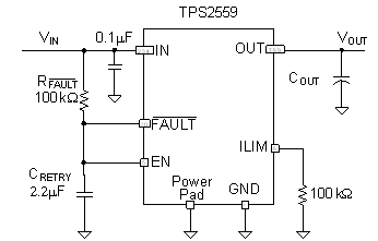
Some applications require that an overcurrent condition disables the part momentarily during a fault condition and re-enables after a pre-set time. This auto-retry functionality can be implemented with an external resistor and capacitor. During a fault condition, FAULT pulls low EN. The part is disabled when EN is pulled below the turn-off threshold, and FAULT goes high impedance allowing C(RETRY) to begin charging. The part re-enables when the voltage on EN reaches the turn-on threshold. The part will continue to cycle in this manner until the fault condition is removed. The auto-retry cycling time is determined by the resistor/capacitor time constant, TPS2559 turn on time and FAULT deglitch time (see Figure 9-13).
 Figure 9-3 Auto-Retry Circuit
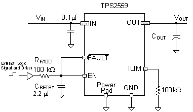
Some applications require auto-retry functionality and the ability to enable/disable with an external logic signal. Figure 9-4 shows how an external logic signal can drive EN through R( FAULT) and maintain auto-retry functionality. The resistor, capacitor time constant determines the auto-retry time-out period.
 Figure 9-4 Auto-Retry Circuit with External EN Signal