SLVS930C December   2009  – October 2020 TPS2560 , TPS2561

PRODUCTION DATA  

  1. Features
  2. Applications
  3. Description
  4. Revision History
  5. Device Comparison Table
  6. Pin Configuration and Functions
  7. Specifications
    1. 7.1 Absolute Maximum Ratings
    2. 7.2 ESD Ratings
    3. 7.3 ESD Ratings: Surge
    4. 7.4 Recommended Operating Conditions
    5. 7.5 Thermal Information
    6. 7.6 Electrical Characteristics
    7. 7.7 Dissipation Ratings
    8. 7.8 Typical Characteristics
  8. Parameter Measurement Information
  9. Detailed Description
    1. 9.1 Overview
    2. 9.2 Functional Block Diagram
    3. 9.3 Feature Description
      1. 9.3.1 Overcurrent Conditions
      2. 9.3.2 FAULTx Response
      3. 9.3.3 Undervoltage Lockout (UVLO)
      4. 9.3.4 Enable ( ENx or ENx)
      5. 9.3.5 Thermal Sense
    4. 9.4 Device Functional Modes
  10. 10Power Supply Recommendations
    1. 10.1 Self-Powered and Bus-Powered Hubs
    2. 10.2 Low-Power Bus-Powered and High-Power Bus-Powered Functions
  11. 11Layout
    1. 11.1 Layout Guidelines
      1. 11.1.1 Power Dissipation
    2. 11.2 Layout Example
  12. 12Device and Documentation Support
    1. 12.1 Receiving Notification of Documentation Updates
    2. 12.2 Support Resources
    3. 12.3 Trademarks
    4. 12.4 Electrostatic Discharge Caution
    5. 12.5 Glossary
  13. 13Mechanical, Packaging, and Orderable Information

Package Options

Mechanical Data (Package|Pins)
Thermal pad, mechanical data (Package|Pins)
Orderable Information

Parameter Measurement Information

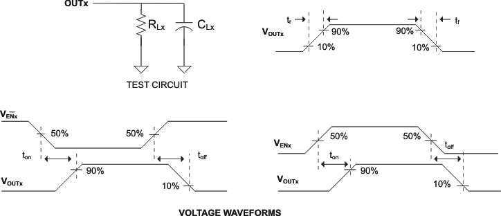
GUID-DDF983A0-2778-402D-BAD7-04B2D3C043E6-low.gif Figure 8-1 Test Circuit and Voltage Waveforms
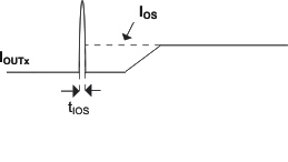
GUID-F7AF8176-5E59-4CE0-AE41-BB16ADCCA3A4-low.gif Figure 8-2 Response Time to Short Circuit Waveform
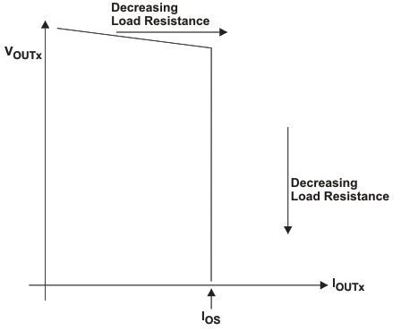
GUID-D4713D74-7352-46E0-BA87-EC97B4B9018B-low.gif Figure 8-3 Output Voltage vs Current-Limit Threshold