SLVSGT8 December   2022 TPS25961

PRODUCTION DATA  

  1. Features
  2. Applications
  3. Description
  4. Revision History
  5. Pin Configuration and Functions
  6. Specifications
    1. 6.1 Absolute Maximum Ratings
    2. 6.2 ESD Ratings
    3. 6.3 Recommended Operating Conditions
    4. 6.4 Thermal Information
    5. 6.5 Electrical Characteristics
    6. 6.6 Timing Requirements
    7. 6.7 Switching Characteristics
    8. 6.8 Typical Characteristics
  7. Detailed Description
    1. 7.1 Overview
    2. 7.2 Functional Block Diagram
    3. 7.3 Feature Description
      1. 7.3.1 Undervoltage Protection (UVP) and Undervoltage Lockout (UVLO)
      2. 7.3.2 Overvoltage Protection
      3. 7.3.3 Inrush Current, Overcurrent and Short Circuit Protection
        1. 7.3.3.1 Slew Rate and Inrush Current Control (dVdt)
        2. 7.3.3.2 Active Current Limiting
        3. 7.3.3.3 Short-Circuit Protection
      4. 7.3.4 Overtemperature Protection (OTP)
      5. 7.3.5 Fault Response
    4. 7.4 Device Functional Modes
  8. Application and Implementation
    1. 8.1 Application Information
    2. 8.2 Typical Application
      1. 8.2.1 Adapter input protection for set-top boxes
      2. 8.2.2 Design Requirements
      3. 8.2.3 Detailed Design Procedure
        1. 8.2.3.1 Programming the Current-Limit Threshold: RILM Selection
        2. 8.2.3.2 Undervoltage and Overvoltage Lockout Set Point
        3. 8.2.3.3 Output Voltage Rise Time (tR)
      4. 8.2.4 Application Curves
    3. 8.3 Application Example
      1. 8.3.1 Application Curves
    4. 8.4 Power Supply Recommendations
      1. 8.4.1 Transient Protection
      2. 8.4.2 Output Short-Circuit Measurements
    5. 8.5 Layout
      1. 8.5.1 Layout Guidelines
      2. 8.5.2 Layout Example
  9. Device and Documentation Support
    1. 9.1 Documentation Support
      1. 9.1.1 Related Documentation
    2. 9.2 Receiving Notification of Documentation Updates
    3. 9.3 Support Resources
    4. 9.4 Trademarks
    5. 9.5 Electrostatic Discharge Caution
    6. 9.6 Glossary
  10. 10Mechanical, Packaging, and Orderable Information

Package Options

Mechanical Data (Package|Pins)
Thermal pad, mechanical data (Package|Pins)
Orderable Information

Description

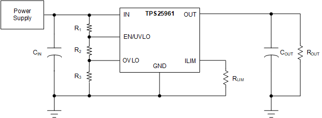
The TPS25961 eFuse (integrated FET hot-swap device) is a highly integrated circuit protection and power management solution in a small package. The device provides multiple protection modes using very few external components and is a robust defense against overloads, short-circuits, voltage surges, and excessive inrush current. Output current limit level can be set with a single external resistor. Inrush current is managed using output slew rate control internally. To protect an input overvoltage condition, the device provides an option to externally set a user-defined overvoltage cutoff threshold or use a fixed internal threshold.

The devices are characterized for operation over a junction temperature range of –40 °C to +125 °C.

Device Information
PART NUMBER(1) PACKAGE BODY SIZE (NOM)
TPS25961DRV SON (6) 2.00 mm × 2.00 mm
For all available packages, see the orderable addendum at the end of the data sheet.
GUID-20220623-SS0I-5DPR-FZBM-TMSVSDWVSK1J-low.gifSimplified Schematic