SLVSGT8 December 2022 TPS25961
PRODUCTION DATA
- 1 Features
- 2 Applications
- 3 Description
- 4 Revision History
- 5 Pin Configuration and Functions
- 6 Specifications
-
7 Detailed Description
- 7.1 Overview
- 7.2 Functional Block Diagram
- 7.3 Feature Description
- 7.4 Device Functional Modes
- 8 Application and Implementation
- 9 Device and Documentation Support
- 10Mechanical, Packaging, and Orderable Information
Package Options
Mechanical Data (Package|Pins)
- DRV|6
Thermal pad, mechanical data (Package|Pins)
- DRV|6
Orderable Information
7.3.1 Undervoltage Protection (UVP) and Undervoltage Lockout (UVLO)
TPS25961 constantly monitors the input supply to ensure that the load is powered up only when the voltage is at a sufficient level. During the start-up condition, the device waits for the input supply to rise above an internal fixed threshold VUVP(R) before it proceeds to turn ON the FET. Similarly, during the ON condition, if the input supply falls below the UVP threshold VUVP(F), the FET is turned OFF. The UVP rising and falling thresholds are slightly different, thereby providing some hysteresis and ensuring stable operation around the threshold voltage.
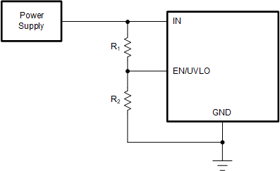
The TPS25961 also provides an user adjustable UVLO mechanism to ensure that the load is powered up only when the voltage is at a sufficient level as per the specific system requirement. This can be achieved by dividing the input supply and feeding it to the EN/UVLO pin. Whenever the voltage at the EN/UVLO pin falls below a threshold VUVLO(F), the device turns OFF the FET. The FET is turned ON again when the voltage rises above the threshold VUVLO(R). The rising and falling thresholds on this pin are slightly different, thereby providing some hysteresis and ensuring stable operation around the threshold voltage.
The user must choose the resistor divider values appropriately to map the desired input undervoltage level to the UVLO threshold of the part.
 Figure 7-1 Adjustable Undervoltage
Lockout