SLVSHR9 December 2024 TPS25984B
PRODUCTION DATA
- 1
- 1 Features
- 2 Applications
- 3 Description
- 4 Device Comparison Table
- 5 Pin Configuration and Functions
- 6 Specifications
-
7 Detailed Description
- 7.1 Overview
- 7.2 Functional Block Diagram
- 7.3
Feature Description
- 7.3.1 Undervoltage Protection
- 7.3.2 Insertion Delay
- 7.3.3 Overvoltage Protection
- 7.3.4 Inrush Current, Overcurrent, and Short-Circuit Protection
- 7.3.5 Analog Load Current Monitor (IMON)
- 7.3.6 Mode Selection (MODE)
- 7.3.7 Digital Overcurrent Indication (D_OC)
- 7.3.8 Stacking Multiple eFuses for Scalability
- 7.3.9 Analog Junction Temperature Monitor (TEMP)
- 7.3.10 Overtemperature Protection
- 7.3.11 Fault Response and Indication (GOK/FLT)
- 7.3.12 Power-Good Indication (PG)
- 7.3.13 Output Discharge
- 7.3.14 FET Health Monitoring
- 7.4 Device Functional Modes
- 8 Application and Implementation
- 9 Device and Documentation Support
- 10Revision History
- 11Mechanical, Packaging, and Orderable Information
Package Options
Mechanical Data (Package|Pins)
- RZJ|32
Thermal pad, mechanical data (Package|Pins)
- RZJ|32
Orderable Information
7.3.5 Analog Load Current Monitor (IMON)
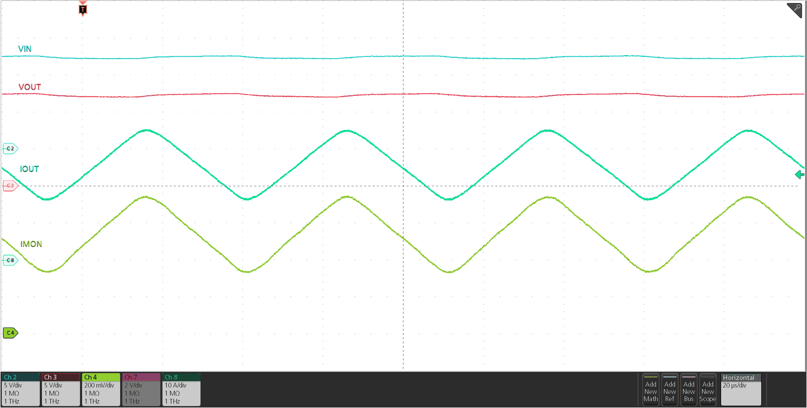
The TPS25984Bx allows the system to monitor the output load current accurately by providing an analog current on the IMON pin which is proportional to the current through the FET. The benefit of having a current output is that the signal can be routed across a board without adding significant errors due to voltage drop or noise coupling from adjacent traces. The current output also allows the IMON pins of multiple TPS25984Bx devices to be tied together to get the total current of the system in a parallel eFuse configuration. The IMON signal can be converted to a voltage by dropping it across a resistor at the point of monitoring. The user can sense the voltage (VIMON) across the RIMON to get a measure of the output load current using Equation 13.
The TPS25984Bx IMON circuit is designed to provide high bandwidth and high accuracy across load and temperature conditions, irrespective of board layout and other system operating conditions. This design allows the IMON signal to be used for advanced dynamic platform power management techniques such as PROCHOT™ or Intel PSYS™ to maximize system power usage and platform throughput without sacrificing safety or reliability.
 Figure 7-6 Analog Load Current Monitor Response
TI recommends using the IMON pin for load current monitoring information only during steady-state. During inrush, the IMON pin reports load current with higher error.
The IMON pins of multiple TPS25984Bx devices can be tied together to monitor the total system current even if the eFuses are operating independently, or in other words not connected together in a stacked or parallel configuration.
- The ILIM pin reports the individual device load current at all times and can also be used as an analog load current monitor for each individual device.
- Care must be taken to minimize parasitic capacitance on the ILIM pin to avoid any impact on the start-up current limit protection and short-circuit protection timing.