SLVSDT4F October 2017 – December 2021 TPS2662
PRODUCTION DATA
- 1 Features
- 2 Applications
- 3 Description
- 4 Revision History
- 5 Device Comparison Table
- 6 Pin Configuration and Functions
- 7 Specifications
- 8 Parameter Measurement Information
-
9 Detailed Description
- 9.1 Overview
- 9.2 Functional Block Diagram
- 9.3
Feature Description
- 9.3.1 Undervoltage Lockout (UVLO)
- 9.3.2 Overvoltage Protection (OVP)
- 9.3.3 Hot Plug-In and Inrush Current Control
- 9.3.4 Reverse Polarity Protection
- 9.3.5 Overload and Short-Circuit Protection
- 9.3.6 Reverse Current Protection
- 9.3.7 FAULT Response
- 9.3.8 IN, OUT, RTN, and GND Pins
- 9.3.9 Thermal Shutdown
- 9.4 Device Functional Modes
-
10Application and Implementation
- 10.1 Application Information
- 10.2 Typical Application
- 10.3 System Examples
- 10.4 Do's and Don'ts
- 11Power Supply Recommendations
- 12Layout
- 13Device and Documentation Support
- 14Mechanical, Packaging, and Orderable Information
Package Options
Mechanical Data (Package|Pins)
- DRC|10
Thermal pad, mechanical data (Package|Pins)
- DRC|10
Orderable Information
6 Pin Configuration and Functions
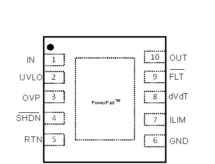
 Figure 6-1 DRC Package10-Pin VSONTop View
Table 6-1 Pin Functions
| PIN | TYPE | DESCRIPTION | |
|---|---|---|---|
| NO. | NAME | ||
| 1 | IN | Power | Input supply voltage |
| 2 | UVLO | I | Resistor programmable undervoltage lockout threshold setting input. An undervoltage event opens the internal FET. If the Undervoltage Lock Out function is not needed, the UVLO terminal must be connected to the IN terminal with at least a 1-MΩ resistor. UVLO pin is 5-V rated and this resistor limits the UVLO pin current to < 60 µA. |
| 3 | OVP | I | Resistor programmable overvoltage protection threshold. An overvoltage event opens internal FET. In TPS26620, TPS26621, TPS26624, TPS26625 devices, if overvoltage protection feature is not to be used then connect OVP terminal to RTN. For overvoltage clamp response (TPS26622 and TPS26623 only) connect OVP to RTN externally. |
| 4 | SHDN | I | Shutdown pin. Pulling the pin low makes the device to enter into low power shutdown mode. Cycling SHDN low and then back high resets the device that has latched off (TPS26620, TPS26622, TPS26624 only) due to a fault condition. |
| 5 | RTN | – | Reference ground for all internal voltages |
| 6 | GND | – | System ground |
| 7 | ILIM | I/O | A resistor from this pin to RTN sets the overload and short-circuit current limit. See the Overload and Short Circuit Protection section. |
| 8 | dVdT | I/O | A capacitor from this pin to RTN sets output voltage slew rate. See the Hot Plug-In and In-Rush Current Control section. |
| 9 | FLT | O | Fault event indicator. This pin is an open drain output. If unused, leave floating. |
| 10 | OUT | Power | Output voltage |
| – | PowerPAD™ | – | Connect PowerPAD to RTN plane for heat sinking. Do not use PowerPAD as the only electrical connection to RTN. |