SLVSE94G September 2018 – June 2024 TPS2663
PRODUCTION DATA
- 1
- 1 Features
- 2 Applications
- 3 Description
- 4 Device Comparison Table
- 5 Pin Configuration and Functions
- 6 Specifications
- 7 Parameter Measurement Information
-
8 Detailed Description
- 8.1 Overview
- 8.2 Functional Block Diagram
- 8.3
Feature Description
- 8.3.1 Hot Plug-In and Inrush Current Control
- 8.3.2 PGOOD and PGTH
- 8.3.3 Undervoltage Lockout (UVLO)
- 8.3.4 Overvoltage Protection (OVP)
- 8.3.5 Input Reverse Polarity Protection (B_GATE, DRV)
- 8.3.6 Reverse Current Protection
- 8.3.7 Overload and Short-Circuit Protection
- 8.3.8 Output Power Limiting, PLIM (TPS26632, TPS26633, TPS26635, TPS26636, and TPS26637 Only)
- 8.3.9 Current Monitoring Output (IMON)
- 8.3.10 FAULT Response (FLT)
- 8.3.11 IN_SYS, IN, OUT, and GND Pins
- 8.3.12 Thermal Shutdown
- 8.3.13 Low Current Shutdown Control (SHDN)
- 8.4 Device Functional Modes
-
9 Application and Implementation
- 9.1 Application Information
- 9.2
Typical Application: Power Path Protection in a PLC System
- 9.2.1 Design Requirements
- 9.2.2 Detailed Design Procedure
- 9.2.3 Application Curves
- 9.3 System Examples
- 9.4 Dos and Do Nots
- 9.5 Power Supply Recommendations
- 9.6 Layout
- 10Device and Documentation Support
- 11Revision History
- 12Mechanical, Packaging, and Orderable Information
Package Options
Refer to the PDF data sheet for device specific package drawings
Mechanical Data (Package|Pins)
- RGE|24
- PWP|20
Thermal pad, mechanical data (Package|Pins)
Orderable Information
8.3.4 Overvoltage Protection (OVP)
The TPS2663x devices incorporate circuitry to protect the system during overvoltage conditions. The TPS26630 and TPS26631 feature an accurate ±2% adjustable overvoltage cutoff functionality. A voltage more than V(OVPR) on OVP pin turns off the internal FET and protects the downstream load. To program the OVP threshold externally, connect a resistor divider from IN_SYS supply to OVP terminal to GND as shown in the Simplified Schematic.
The TPS26630 and TPS26631 also feature a factory set 34.3-V input overvoltage cutoff V(IN_SYS_OVP) threshold with a 440-mV hysteresis. This feature can be enabled by connecting the OVP terminal directly to the GND terminal. The TPS26632, TPS26633 and TPS26636 feature an internally fixed 35-V maximum overvoltage clamp V(OVC) functionality. The TPS26632 and TPS26633 clamps the output voltage to V(OVC) when the input voltage exceeds 35 V. TPS26635 features a fixed 39-V maximum overvoltage clamp level. During the output voltage clamp operation, the power dissipation in the internal MOSFET is PD = (V(IN_SYS) – V(OVC)) × I(OUT). Excess power dissipation for a prolonged period can increase the device temperature. To avoid this increase, the internal FET is operated in overvoltage clamp for a maximum duration of tOVC(dly), 162 ms (typical). After this duration, the internal FET is turned OFF and the subsequent operation of the device depends on the MODE configuration (auto-retry or latch-off) setting as shown in Table 8-1.
Figure 7-1 shows the turn-ON behavior when OVP pin voltage falls below V(OVPF) threshold.
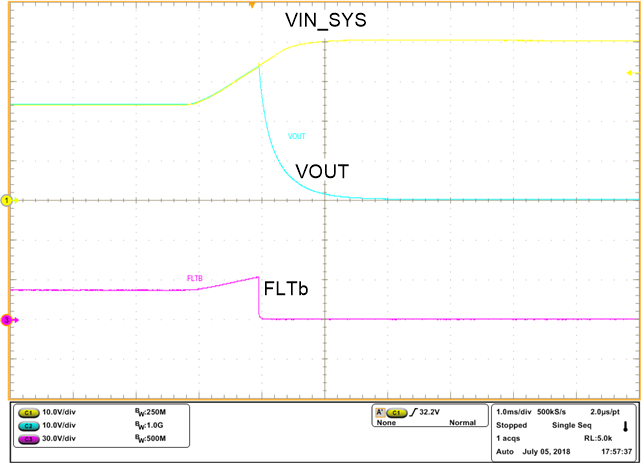
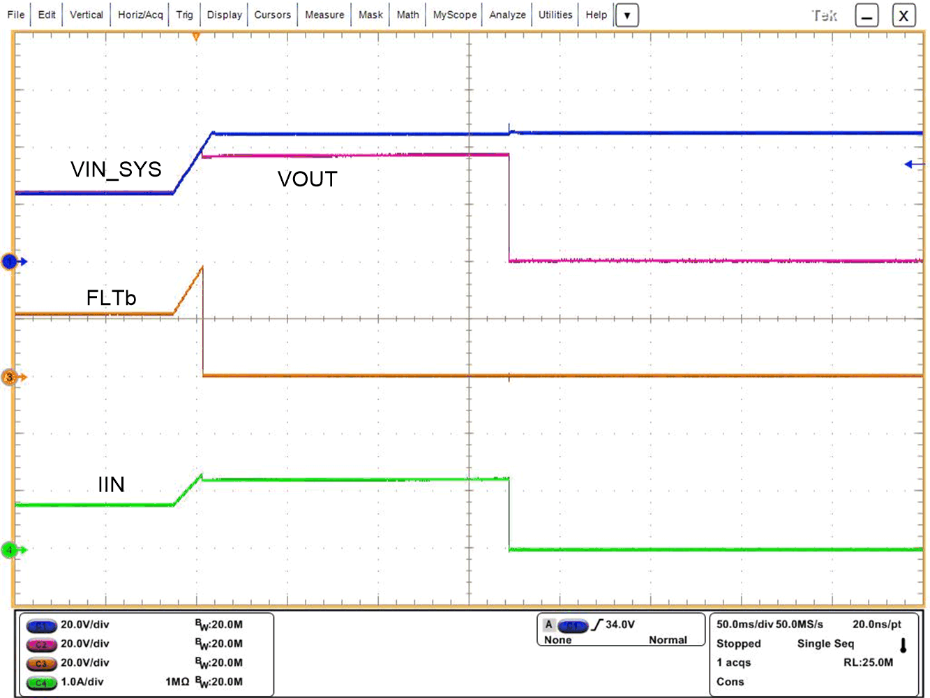
Figure 8-5 illustrates the overvoltage cutoff functionality and Figure 8-6 illustrates the overvoltage clamp functionality. FLT is asserted after a delay of 617 µs (typical) after entering in overvoltage clamp mode and remains asserted until the overvoltage fault is removed.

| TPS26630 and TPS26631 | ||

| TPS26635 | RLOAD = 30 Ω, FLT connected to VOUT | |